| PCG700 Programming
HAL Laboratory
|
|||||||||||||||||||||||||||||||||||||||||||||||||||||||||||||||||||||||||||||||||||||||||||||||||||||||||||||
| General | |||||||||||||||||||||||||||||||||||||||||||||||||||||||||||||||||||||||||||||||||||||||||||||||||||||||||||||
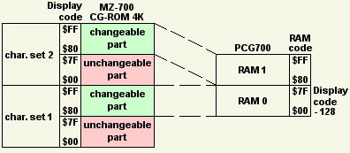
The RAM of the PCG700 allows to modify up to 256 characters of both character sets. The PCG700 can process only the upper 128 characters of each character set. The lower 128 characters of each character set cannot be modified by the PCG700. This means that the character codes $00 - $7F of each character set cannot be changed - they remain always active; but the character codes $80 - $FF can be changed.
As known, the MZ-700 has two character sets, each having 256 characters.
Both character sets reside in one ROM chip having a capacity of 4 kb.
If you compute: The 256 characters of the PCG700 use: If you use a special programming technique then all dots of the screen can be set as needed by modifying each character matrix to be displayed on the screen. The advantage of this method ( point-to-point-positioning control / control of a single dot ) is it is much more faster than a bitmap graphic, because the CPU moves 64 bytes in a single step ( bitmap graphic only 8 bits ). And, you do not have to solder anything or to cut wires, copper tracks, etc. on the MZ-700's board. The HSW-switch must be in the position PCG ( ON ) and the jumper SSW must be set to the position "ON". This enables the PCG700 to be controlled by software. For more information about the setting of the jumpers and switches read "PCG700 Operation" now. The PCG700 uses memory mapped I/O to be controlled by software. This
means, the software uses simple I/O commands to control the PCG700.
The ports exclusively used for all functions are $E010, $E011, and $E012.
|
|||||||||||||||||||||||||||||||||||||||||||||||||||||||||||||||||||||||||||||||||||||||||||||||||||||||||||||
| Ports control | |||||||||||||||||||||||||||||||||||||||||||||||||||||||||||||||||||||||||||||||||||||||||||||||||||||||||||||
|
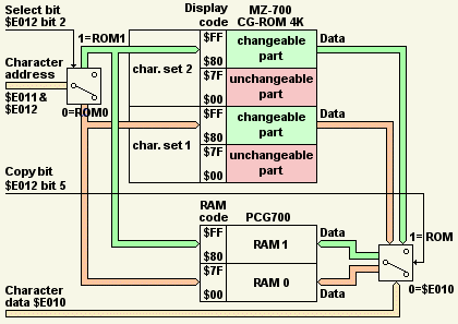
Port $E012 is used to control the PCG700. All bits are write only. The meaning of the control bits follows:
|
|||||||||||||||||||||||||||||||||||||||||||||||||||||||||||||||||||||||||||||||||||||||||||||||||||||||||||||
| Using the PCG700 from BASIC | |||||||||||||||||||||||||||||||||||||||||||||||||||||||||||||||||||||||||||||||||||||||||||||||||||||||||||||
|
All codes written in BASIC DATA lines are: DATA 16, 126, 20, 62, 85, 73, 50, 0 ( decimal ) or DATA $10, $7E, $14, $3E, $55, $49, $32, $0 ( hexadecimal ) |
|||||||||||||||||||||||||||||||||||||||||||||||||||||||||||||||||||||||||||||||||||||||||||||||||||||||||||||
| How to program the PCG700 by BASIC | |||||||||||||||||||||||||||||||||||||||||||||||||||||||||||||||||||||||||||||||||||||||||||||||||||||||||||||
|
The following HuBASIC program transfers the character from the example shown above into the PCG RAM0:
In this example the display code 239 shall be modified ( BASIC line 20 ). The RAM0 shall be used ( RAM address area 0 - 128 ). To this the value 128 is to be subtracted from the character code 239 ( line 30 ). 239 - 128 = 111. The first address in RAM0 is computed by 111 * 8 = 888; the last is 111 * 8 + 7 = 895 ( line 50 ). The data must be transferred by the port $E010 ( line 70 ) and is read prior the transfer into the variable A by line 60 ( data are defined in line 130 ). The RAM0 is addressed by computing the address in the variable AD into
a lower and upper part ( lines 80 and 90 ). The lower part is written
into the port $E011 by line 80; the upper part by line 90. The PCG is
informed that all data written to its ports are now valid by setting
the strobe bit 4 ( line 90: by adding 16 ). The programming of the PCG
is finished by resetting the strobe bit 4 by line 100. The following HuBASIC program copies one character from the MZ-700's CG-ROM into the PCG RAM0:
This example copies the character related to the display code 263 from ROM0 into the PCG RAM0. It is very similar to the previous example except that the copy bit 5 is set by line 70. Adding of 32 invokes the copy process. The following HuBASIC program transfers 256 characters into the PCG RAM0:
|
|||||||||||||||||||||||||||||||||||||||||||||||||||||||||||||||||||||||||||||||||||||||||||||||||||||||||||||
| How to program the PCG700 by Assembler | |||||||||||||||||||||||||||||||||||||||||||||||||||||||||||||||||||||||||||||||||||||||||||||||||||||||||||||
|
For both examples the accumulator register A must be set to the display code prior to the call of the routines. This code has the same value as the PCG700 RAM code or the CG-ROM0 code of the MZ-700 ( in example 2 ). Both routines are designed in that way so that you can use directly the display code ( $80 - $FF ) or the computed PCG700 RAM0 code ( = display code minus $80 ). No matter which code you use, both codes will be addressed correctly. ; PROGRAM 1 CHARACTER FROM YOUR MATRIX TABLE INTO PCG700 RAM0
; A = DISPLAY/RAM CODE ( can be e.g. 239 or 239-128=111... )
; HL = POINTER TO YOUR MATRIX TABLE IN THE MZ-700 RAM
F5 PRG1CH: PUSH AF ; save display/RAM0 code
E5 PUSH HL ; save HL ( HL will be used next )
E5 PUSH HL ; save me the matrix table pointer
87 ADD A,A ; multiply by 2
6F LD L,A ; get result into register L
2600 LD H,0 ; init H
29 ADD HL,HL ; multiply by 2 = x4
29 ADD HL,HL ; multiply by 2 = x8 it is now the
; absolute PCG700 RAM0 address
EB EX DE,HL ; get address into register DE
E1 POP HL ; get address of your matrix table
0608 LD B,8 ; init DJNZ counter for 8 matrix bytes
7E P1CH1: LD A,(HL) ; get 1 byte of your matrix table
3210E0 LD ($E010),A ; output matrix byte by port $E010
7B LD A,E ; get lower address into register A
3211E0 LD ($E011),A ; output lower address by port $E011
7A LD A,D ; get upper address into register A
C610 ADD 16 ; add strobe
3212E0 LD ($E012),A ; output all to port $E012
7A LD A,D ; prepare A
; to close operation of 1 matrix byte
3212E0 LD ($E012),A ; reset strobe ( closes operation )
13 INC DE ; PCG700 RAM0 matrix table pointer + 1
23 INC HL ; pointer + 1 for your matrix table
10EA DJNZ P1CH1 ; process next matrix byte if any
E1 POP HL ; restore HL ( to callers contents )
F1 POP AF ; restore AF ( to callers contents )
C9 RET ; goback to caller
The following example copies one character from the MZ-700's CG-ROM0 ( character set 1 ) into the PCG700 RAM0. If you want to copy from the CG-ROM1 ( character set 2 ) into the RAM1 then additional you have to set bit 2 of the port $E012 prior to the output to this port. To this e.g. you can modify the instruction ADD 48 to ADD 52. ; COPY 1 CHARACTER FROM MZ-700 CG-ROM0 INTO PCG700 RAM0
; A = DISPLAY/ROM0/RAM0 CODE ( can be e.g. 239 or 239-128=111... )
F5 COP1CH: PUSH AF ; save display/ROM0/RAM0 code
E5 PUSH HL ; save HL ( HL will be used next )
87 ADD A,A ; multiply by 2
6F LD L,A ; get result into register L
2600 LD H,0 ; init H
29 ADD HL,HL ; multiply by 2 = x4
29 ADD HL,HL ; multiply by 2 = x8 it s now the
; absolute ROM0/RAM0 address
EB EX DE,HL ; get address into register DE
0608 LD B,8 ; init DJNZ counter for 8 matrix bytes
7B COP1C1: LD A,E ; get lower address into register A
3211E0 LD ($E011),A ; output lower address by port $E011
7A LD A,D ; get upper address into register A
C610 ADD 48 ; add strobe & copy flag
3212E0 LD ($E012),A ; output all to port $E012
7A LD A,D ; prepare A
; to close operation of 1 matrix byte
3212E0 LD ($E012),A ; reset strobe ( closes operation )
13 INC DE ; matrix table pointer + 1
10EA DJNZ COP1C1 ; process next matrix byte if any
E1 POP HL ; restore HL ( to callers contents )
F1 POP AF ; restore AF ( to callers contents )
C9 RET ; goback to caller
( Special thanks to Hideki / Japan for the translations from the PCG700 Manual ) More about the PCG700: |
|||||||||||||||||||||||||||||||||||||||||||||||||||||||||||||||||||||||||||||||||||||||||||||||||||||||||||||