So let´s now investigate the
functions within the Interfacecard.....
again we will first display the plan of the components splitted in
function groups and then we´ll display the
related circuitplan marked up with the same function groupd and the same
numbering.
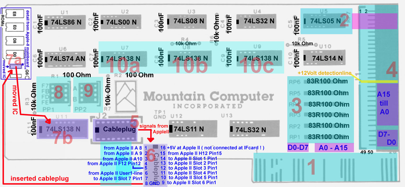
Before we start with examination of the circuitplan and the electronical
part of the unit let´s take a short close view to the 1 part of
the connection between
the interfacecard and the Apple II - in this very case the 16 pin
flatribboncable and the mainboard of the Apple II. The conection
is performed in 2 steps:
1) unplugging the 74LS138 in the position just besides of the D0 ROM ( 7a
)and plugging it in the position of U11 ( 7b ) on the
interfacecard. In the picture
below i inserted a small detail view of the
Apple II mainboard numbered as 7a.
2) then the flatpincable that is pluged in at the J2 position ( 5 ) is
also plugged in at the position where the 74LS138 has been
unplugged. You must
pay attention that pin 1 ( at 5 -J2 ) within the
flatribboncable is connected again in that socket to pin 1 ( at
7a ).
In general you may just assume that the IC hac been relocated to the
Interfacecard and most signals are redirected back to the Apple
II. I listed the
signals present at the IC and "looped through" back to the socket ( 7a )
in the part of number 6. All signals listed as "to Apple II" are
that signals looping
back to the mainboard. The signals labeled as "from Apple II" are also
looped back to the Apple II but they are also used within the
interfacecard.
A remark to the notation: from Apple II H12 pin 16 marks the
location of the IC at the Apple II mainboard - means
Apple II Mainboard position H12 and at
that IC, pin 16. In fact the interfacecard uses the signals
from the cableplug socket from pin 4,5,6 and 15.
| |
 |
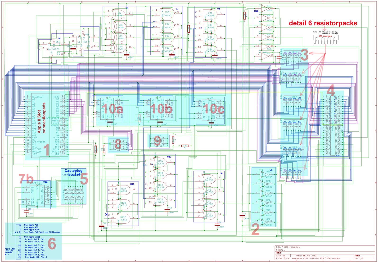
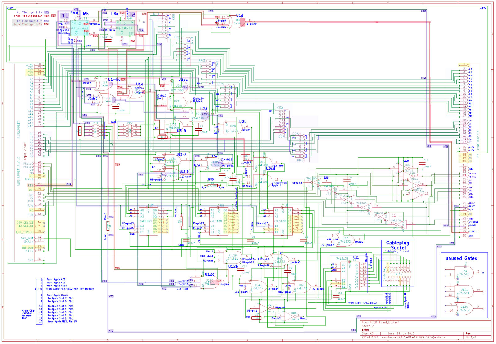
Now we can start comparing the
first function groups in the card and at the circuitplan. In the
circuitplan i have marked the datalines in light violett and the
adressing-lines in blue. Yoe will recognize that this lines pass through
the entire card from the slot connectionpads ( 1 )
entering the resistornetworks ( 3 )
and then end at the connector ( 4 ) which lead by the 50pin
flatribboncable straight to the MCEB box. So in general that
lines are just looped through the card.
Only for very specific operations some of the lines are used also within
the card and some of the lines have splitting knot to branch off
also into the logic of
the card. That part will be discussed later in the page. Just plaes also
recognize that the resistorpacks used on this card are not
common "pullup" networks.
but instead resistors bundled in packs but eash resistor single. These
resistors are used to operate as "impandance" resistors to
optimize the transmission
of the signals while they pass within that long flatribboncable.
| |
 |
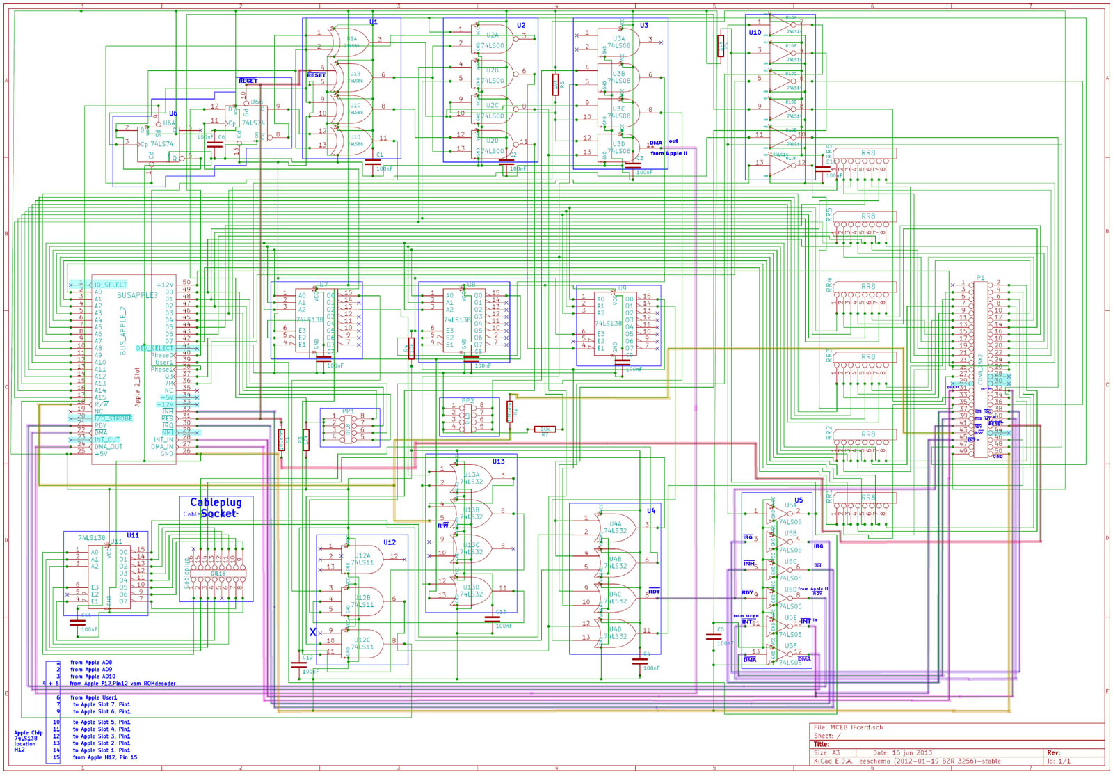
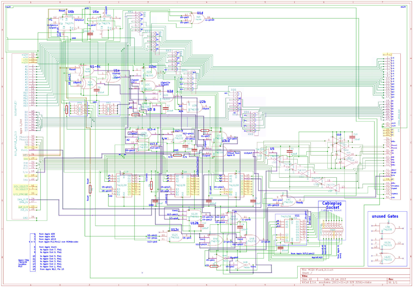
Allthough i haven´t marked
the function groups in the next circuitplan the same function
groups are valid like in the circuitplan above. The difference
in the plan
below i have marked a group of the "control-lines" ( using the same
term like i used in the last page explaining the box ) and a
quite large group of this lines also
are just looped through the card starting from the connectionpads
at the slot and the running up straight to the IC U5 ( marked
with the red 2 in the plan ) and
then passed over to the 50-pin connector at the backpanel of the
card where the 50-pin flatribboncable leads them to the MECB
box. The IC U5 just acts as a
kind of "amplifier" and strengthens the signals before they anter
the cable. Here is the same valid as explained above with the
datalines and the adressing lines:
some of them have "split off knots" and lead selected signals in
the card to for use within the logic of the card. This parts
will be examined next.
| |
 |
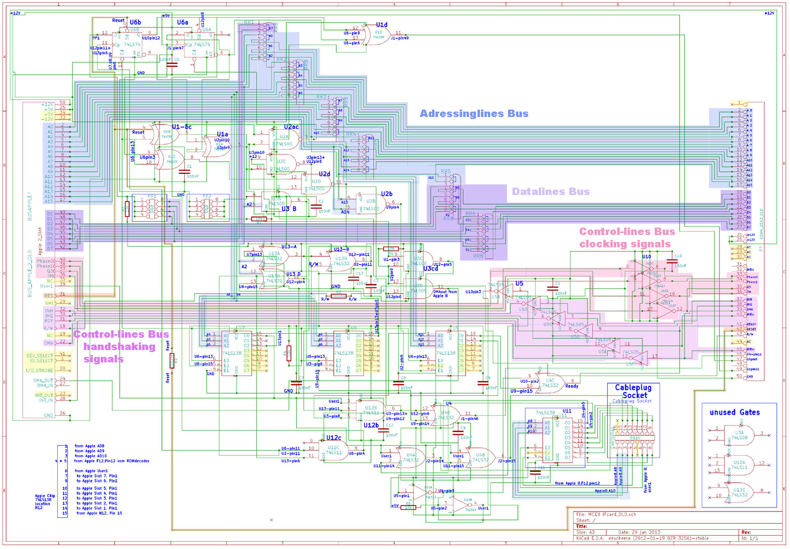
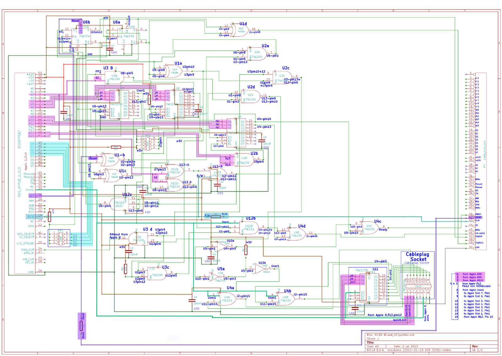
The next point to examine
in the new re-arranged circuitplan will be again the busses at
the interfacecard - but this time the parts like
resistornetworks
and gates of IC´s which are directly integrated in the path of the
busses have been relocated to reside within the bus-paths. This
way we can see what is
not related to the bus-paths. The adressingbus is marked up in blue
color and the related resistor networks are kept in the path.
The databus is marked
in violett color an also there the related resistor networks are
kept within the databuspaths. Parts of the controlbus lines have
been splitted apart, due to their
functions - in this case the clocking signals are collected to one
group and marked with pink color. The handshaking signals (
those that determine the interaction
of communication between the MCEB box and the Apple II ) have been
asumed to a fourth group and marked in darker shaded pink. Lines
not used or connected
are marked with light yellow. The reset-line has been marked in
light red color.
| |
 |
The next point to examine
are the 2 JK FlipFlops within the 74LS74. Each of them is used
to handle timing issues, that can be viewed as a kind of
triggered unit that sends a signal until one of the inputs resets
the unit. So each of this timingunits may be operated
indenpendent from the other unit.
But in this case the second unit may be triggered from the first
unit in aome circumstances. And at the IC U1 at gate d both
signals are collected for
genarating a combined signal if both units result to a preset
condition. I have marked only the lines related to the 2
timingunits and labeled them as
">T1"
and ">T2"
for the lines leading to the units where ">T1"
lead to the first unit and ">T2"
lead to the second unit both Inputline groups are marked
up in blue. The lines that result as output are marked in red color
and they are labeled as "T1>"
if they result from the noninverting output of unit 1 and
as "T1>"
if the have origin from the inverting output. At Unit 2 only the
inverting output is used and marked as "T2>"
while the noninverting output was
not used.
| |
 |
The next point to examine in
the following picture is an examination of those gates that have
been used "for other purposes" which i usually call the
"knitting logic".
In modern circuits this kind of logic is often collected in a
single pal chip. It´s a kind of "switching logic" that
determines the "action" of the card dependent to the
"status" of a group of input lines.
Just for an example:
Only if inputs A
and E
and F are
high and
Inputs B and
C and
D are low
then the common output G of all
gates will
switch to high and
enable a communicationline from
Direction right to direction
left.
| |
 |
In this next picture the lines discussed
previously have been removed.... this permits far more
readability for the rest of the circuit and this remaining
"logic knitting" by the remaining circuits can now be easily
examined. Some of the powerlines +5V and GND have been left in
the picture because some
of the lines within the logic have been tied up to the +5V using a
so called "pullup-resistor" and some are tied directly to GND.
only few resistors have
been used as so called "impendance resistors" in lines running
along the "long path" by the 50 pin flatribboncable. In the
previous pictures the dataline-
bus and the adressinglinebus have been displayed in general while
passing along through from the IFcard to the rear 50 pin
connector to the MCEB. Therefor
in this picture the display of the busses has been reduced to the
remaining lines "split off" and used within the logic. I have
marked 3 lines of special interest:
the reset line, the User1 line and the Read/Write line ( R/W
). I have left the U6 ( 74LS74 ) within the picture because it
is very close "knitted" within the logic
and is very important for timing portion of the logic.
| |
 |
to be continued...
|