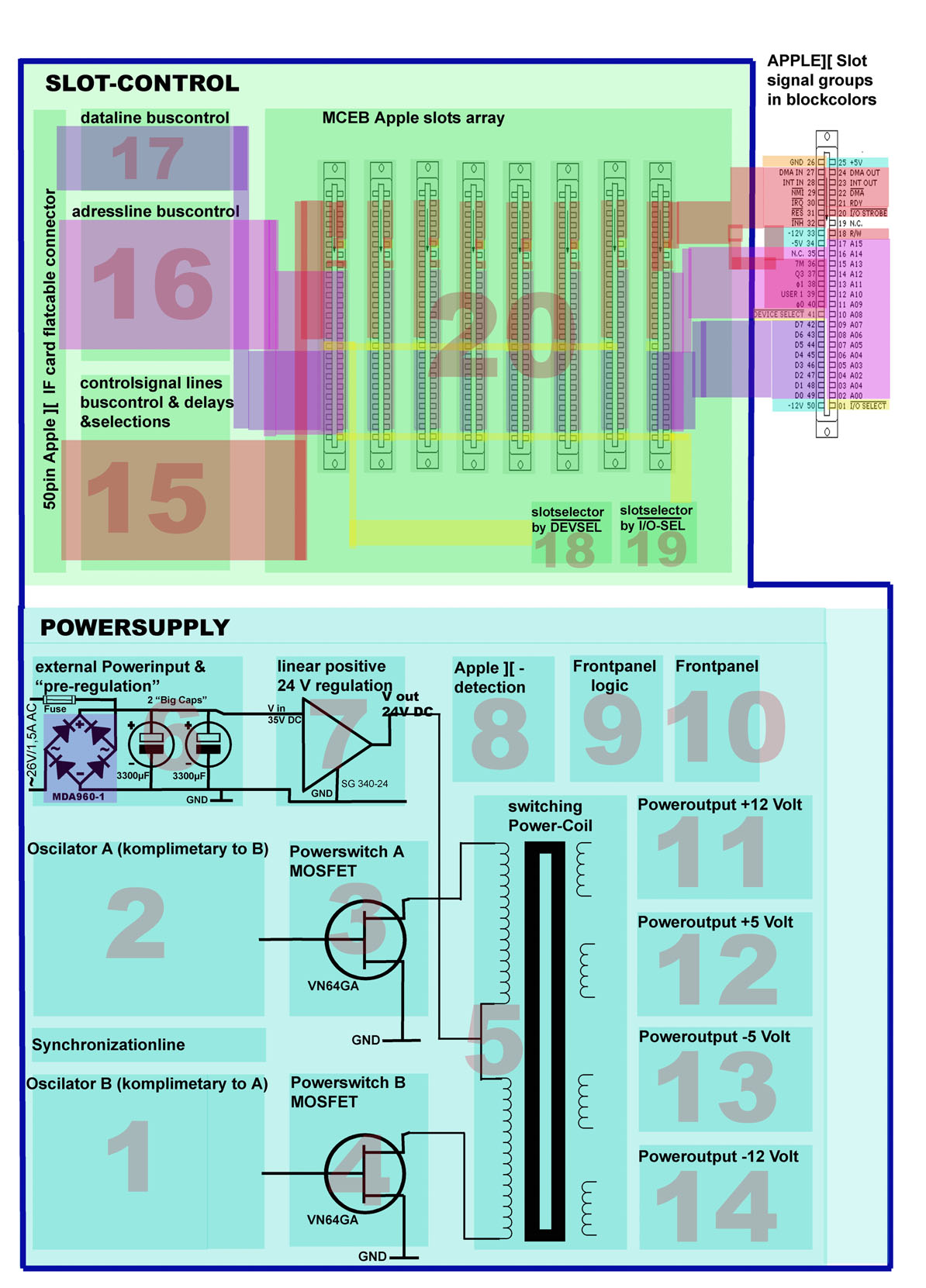
Within the this following section the "applepart" ( the
upper part in the drawíngs enlighted with light green ) of the
box will be explained.
In general you may state that the green enlighted area is a nearly exact
copy of the Apple II with it´s slot area ( part 20 ). The entire
siganls are leaded
from the interfacecard by the 50pin flatribboncable to rhe expansion box
and decodes there in nearly same manner like in the Apple II.
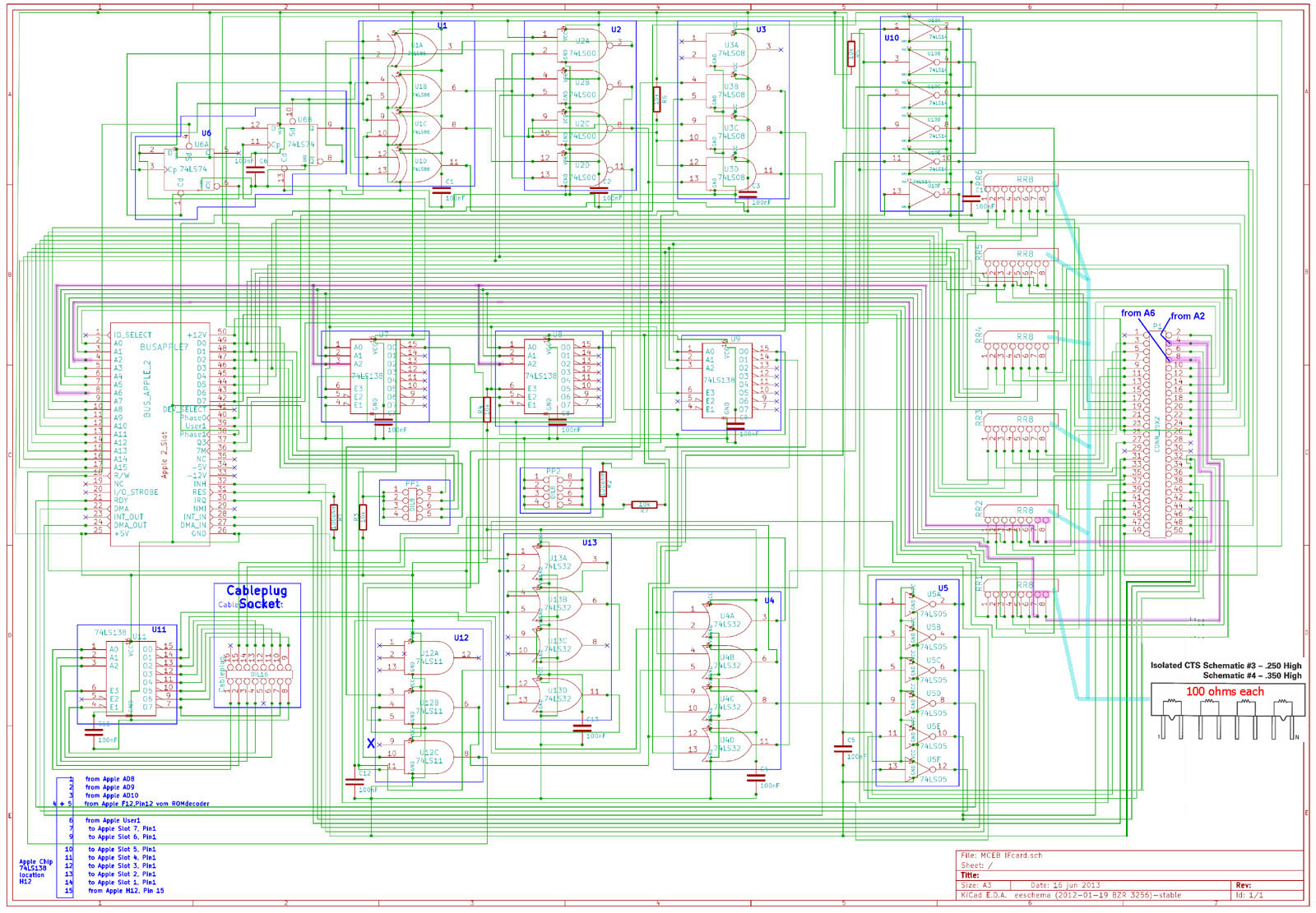
Let´s start examining the details - starting with part 17 - which
controls the databus. The databus consists from the datalines D0
to D7. They enter the box at the flatribbon
cable to the connector J1. Then they are handed passing the pullup
resistor network RP6 to the IC U6 which is a tristate device.
This means, if pin 19 ( CE = Chip enable )
is pulled high to +5Volt the chip acts like an open valve permitting the
flow of data in both directions. the direction of the flow is
controlled by pin 1 ( DIR ) which determines
if the flow is from connector to slot ( Dir B > A equal to read operation
) if the pin 1 gets 0 Volt or from slot to connector ( DIR A > B
equal to write operation ) if at pin 1
gets + 5 Volt. If pin 19 drops to 0 Volt the chip changes to "tristate"
mode and acts like a closed valve with no transmissions in any
direction and by that the
slots in the expansion box get "invisible" to the Apple II ( which will
happen if at the box the "deselect" is active status.
This description is valid the same way to the adressing bus ( represented
by part 16 ) - with the assignments of the "lower" part of the
adressing bus represented by the
adressinglines A0 to A7 which pass the pullupresistor network RP4 and
then get controlled by U4. And the "upper" part of the adressing
bus represents the
adressinglines A8 to A15 which pass the pullupresistor network RP5 and
the IC U5.
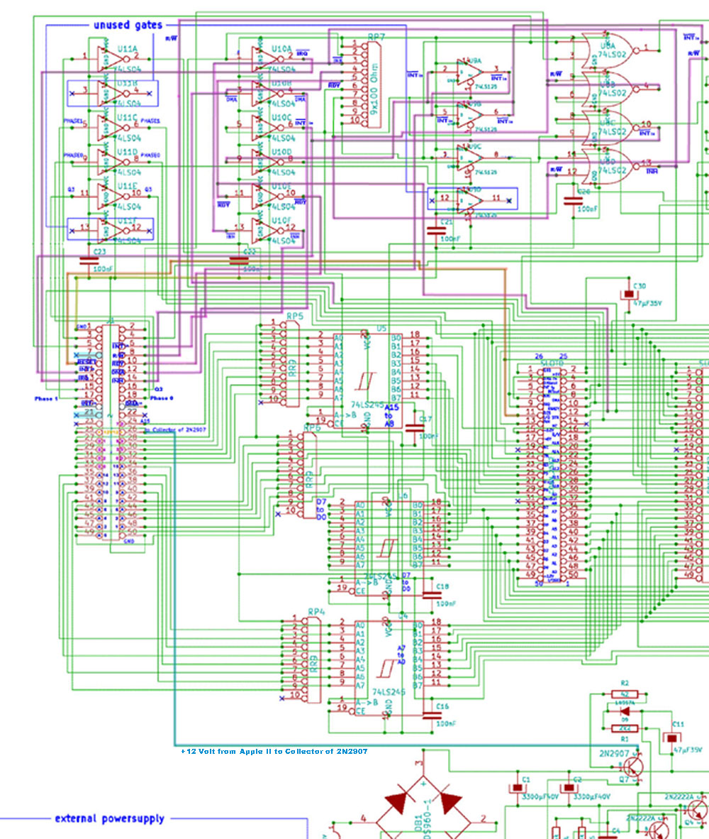
Just to explain the point about the "loop through" logic i now will
show the "other side of the coin" the IFcard of the MCEB and the
data lines ( in light violett )
and adressinglines enlighted with light blue color in the
circuitplan and you can see this lines just running through up
to the "impendancy" resistorpacks
and from there directly to the connector where the flatriddoncable
just passes that lines along to the box:
 |
If some of that
lines are used for decoding within the IFcard they just get a
"split-off" leading to the chips.
The slotselection logic ( which determines which of the 8 slots is
selected at the moment ) is performed by the part 18 and part
19. both are decoder chips that
select 1 line from 8 depending to the input of 3 bits ( pin 1 to 3
) resulting from the adresses of the "soft switches" in
adressing space while the box is active in
"selected" mode. Part 18 ( U2 ) generates the Device select signal
to pin 31 of each single slot while simultanously IC chip U3
generates for each slot the
I/O select signal in part 19. Both chips are linked at pin 1 to 3
together to ensure that each time a slot is selected the same
slot recieves both signals simultanously.
The input pins 4, 5 and 5 ( E1 to E3 ) get control from the
controlline logic in the rear back of chips close to connector
J1 to ensure that slots only get activated,
if the box is in "selected" status and the Apple II wants to access
a slot. Otherwise if the expansionbox is deselected, one of that
controlling lines from pin 4 to
pin 6 changes status and disables the decoding in the chip and sets
the chip to inactive mode. One important remark: this part of
the slot-logic is firmly
connected to the Chip U11 and the 16pin flatribboncable at the
Interfacecard so if the powersupply of the expansionbox is O.K.
and the Apple II is O.K. the
communication between this parts 18 and 19 as well as the part of
U11 at the interfacecard of the box should be one of the first
things to check out for malfunction.
They are essential for the Apple II to select access to the slots
within the computer or at the expansionbox !
Explaining all controlline signals in part 15 in
depth would surely burst any kind of limits within the pages. I
therefor in such a case urgently demand to download
the book
"THE APPLE II CIRCUIT
DESRIPTION" from Winston D. Gaylor. The link is set
here within the title of that book. You may also instead visit
the Apple
Documentation Center at the page:
http://mirrors.apple2.org.za/Apple%20II%20Documentation%20Project/Books/
and pick up from there tha book ( listed in
last position on that page ) - hint: use fast internet
connection... the PDF-file of the book is sized 33 MB ! Before
continueing here with the explenation i advise
you to read the chapter 6 and 7 starting from page 58 in book
( page 60 in PDF-file ) till 64 in book ( page 66 in PDF
file ) and 66 in book ( page 72 in PDF file )
till page 74 in book ( page 80 in PDF file ) and the pages of
chapter 7 up to 99 in book ( page 105 in PDF file )
focused to the slot and its signals.
Alternatively you may instead choose to read
"Understanding the Apple II"
from Jim Sathers the 15th book in the list
of that same page at the Apple Documentation
Center as listed above:
http://mirrors.apple2.org.za/Apple%20II%20Documentation%20Project/Books/
. But also here is the hint valid: use fast internet
connection...
the PDF-file of the book is sized 80 MB ! Within that book
it´s chapter 7 starting at page 157 within the PDF file
and continued till page 165 in the PDF file and then
again starting at page 173 in the PDF file up till page 177 in the
PDF file to get familiar with !
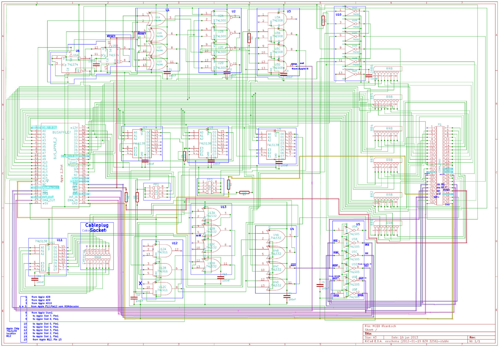
The "Riddle" posted in AF:
You may choose from which of the two sources you
want to recieve the intimate knowledge about the controlsignals
and how they operate within the Apple II.
The same functions are repeated within the expansion box with only
minor changes. But´s exactly the differences we want to examine
here now for better
understanding "how the box" is operated ! Just to spot it out the
main difference is how the signals in part 15 are linked /
interact with the 4 lines that come
from the NE555 ( U1 ) in the front right corner of the box and that
do the handling of the select/deselect switch !
And to list the suspicious cadidates here exactly at the wall in
line up:
No. 1 - From the switch passing at the one end in the brown cable
pin 1 at the connector J3 and the one end of the resistor R13
==> running straight ahead to pin 13 of U7 in the "control
function block" !
No. 2 - starts at the middle of the select /
deselect switch running within the red cable to pin 2 of the
connector J3 passing at one end the resistor R14 and
==> then straight ahead to pin 9 of the U7 in the "control
function block" !
No.3 - starting at the Reset pin4 of the NE555 ( U1 ) and
running straight ahead ==> to pin 1 of the U10 linked there
together with the READY signal !
and of course "candidate"
No.4 - starting at pin 7 of U1 ( DIS ) passing the point
where the resistors R17 an R18 are linked together and then ==>
running straight ahead to pin 6 of U8
within the "control function block" !
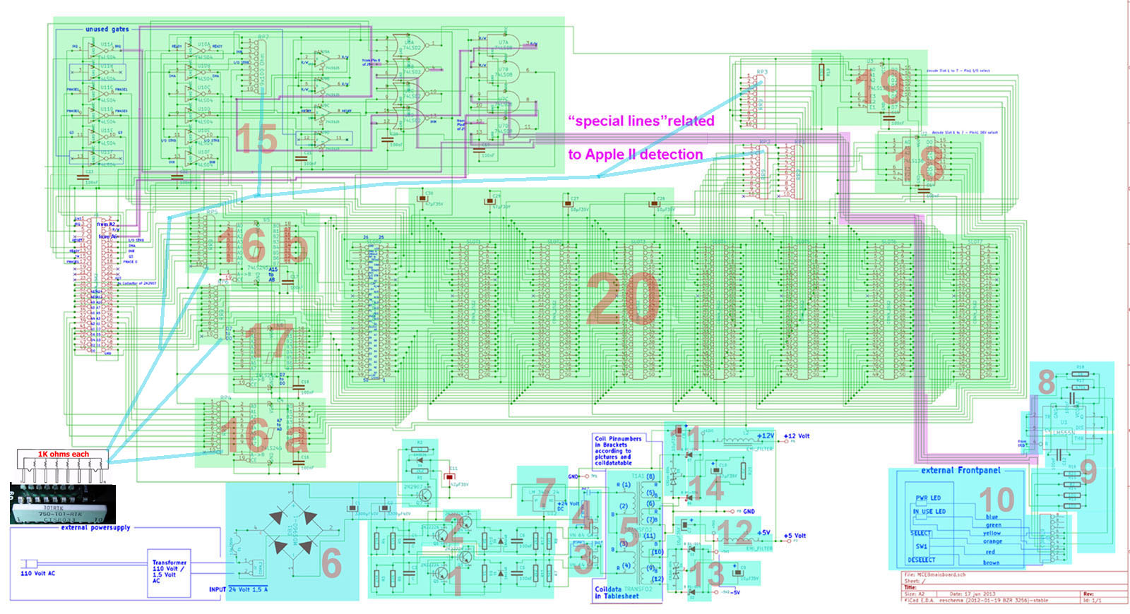 |
In this picture
above i have transferred the markings of the function blocks to
the "real" circuitplan, using the same numbering as in the
previous block plans.
I have marked the 4 previously mention lines as "special
lines" and marked them with light violett enlighting for better
contrast and tracability.
By these 4 "links" to gates of ICs within the "control
function block" part 15 the switches are connected directly to
the part of the box that control the "action"
of the expansion box !
2 of the lines can be traced up till to J1 where the
flatribboncable from the Interface card is ending. Tracing this
2 lines back along within the MCEB interfacecard
you might view that traces within the MCEB interface
card back to the slotconnections in the Apple II and thereby
find out that their origin are the adressinglines A2 and A6 !
When that adressinglines arrive along the flatribboncable the
MCEB bos they are directed to the controlline functionblock and
"knitted" to a logic the permits the
Interface card and the box determine if the box is in
"selected" status or not. I also marked that ovvious lines in
the plan bellow with violett enlighting.
 |
At the moment a have not
analized thst 6 lines and their function in depth, but at least
one thing is for sure at the moment: they are related to the
"soft switches"
within the Apple II memory and parts of the logic "knitted
together" in the MCEB Interfacecard.
Here is the end of the "Riddle-part".
This "control-signal function block" numbered as
part 15 contains the ICs U7 to U11 !
As explained above before the large bunch of
signals within the databus and the adressing bus can be judged
as a kind of "loop through" starting at the
mainboard of the Apple II and it´s CPU entering the interfacecard
in the slot, passing resistor networks that operate as
"impencance load" - without any further
contact to the IC´s mounted at the interfacecard and then slipping
along the 50 pin flatribboncable straight ahaed to the J1
connector in the expansion box
- passing by the bus-control chips U4, U5 and U6 and handed then
straight to the slots within the expansion box. The IC´s U4 to
U6 just control direction of
the signals and decide if they are to be made "insible" to the
Apple II and the interface cards inserted in the expansion box
dependent to the position / status
of the select / deselect switch in the box.
We now can devide the control-signals that are handled within the
"control function block" ( part 15 ) into two groups:
signals that are just passed along like a loopp through
and signals that have to be treated with a kind of "processing" by
getting delayed, inverted or connected for logic interaction.
Within the first group the "clocking"-signals of:
7M,
Q3,
Phase 0 and
Phase 1´are treated as "loop through".
This signals just pass an "driver" targeting to
strengthen the signal after it´s "weakening" long journey made
from the Apple II passing the
interfacecard and the flatribboncable before it´s handed to the
expansion box slots.
Phase 0 enters - after entering the
box at J1 - at pin 9 the IC U11 and leaves it at pin 8 into the
box.
Phase 1 enters - after entering the
box at J1 - at pin 5 the IC U11 and leaves it at pin 6 into the
box.
Q3 enters - after entering the box at
J1 - at pin 11 the IC U11 and leaves it at pin 10 into the box.
7M enters - after entering the box at
J1 - and jumps directly - without any kind of "freshen up
procedure" by any IC - into the box.
The signals INTin
and INTout are used as a
daisychain same like DMAin
and DMAout with
the same logic like in the Apple II:
DMAin DMAout
-----------DMAin
DMAout -----------DMAin
DMAout -----------DMAin
DMAout -----------DMAin
DMAout -----------DMAin
DMAout
INTin INTout----------------INTin
INTout----------------INTin
INTout----------------INTin
INTout----------------INTin
INTout----------------INTin
INTout--
the signals:
R/W
well the R/W
line is used to of course to determine read
or
write oparations to the
interface cards.... but in practical use within the box
this line is used to control the chips and control the bus by
setting the lines to operate in the one or other direction. If
Write
operation is
demanded this line is pulled to low if Read
operation is to be performed this line remains high.
I/O STROBE
is one of the handshake lines. If set
to low it indicates that at the interface card is valid
information present at the bus. This signal
controls the synconization of the 2 following handshakelines by
issueing a Strobe-signal which is a
short drop from high to low.
IRQ
this signal is pulled down to low from the interfacecard if it
damands that the CPU shall listen to an inquiry from the card.
( IRQ
= Interrupt
Request
)
READY
this signal is pulled to high if the
CPU tells the card that the CPU will listen to it.
( READY ... to listen...
)
DMA
if a card in one of the slots, has a own CPU and that CPU at the
card wants to access the memory of the Apple II, then that
"card-CPU" will pull down this line to low and the CPU in the
Apple II will recognize and grant this access to it´s memory
(
DMA = Direct
Memory Access
)
INH
The
INHIBIT line is a very
special kind of "blocking"-line. It can be pulled down by either
a interfacecard or the Apple II and the
device, that pulls the line down to low blocks the access of any
other one of the devices to access any parts of the computer.
RES
If the
resetline is pulled down to
low by either the Apple II or any of the interface cards, then
the entire systems are set back to the
very initial status just after the system has been powered up.
When this line is pulled - any kind of
operation that has been performed
before the line has been pulled - will be terminated immediatly.
NMI
this signal is very similar to the reset signal, with one very
difference: the reset signal sets all counters to "0" while
NMIsignal
leaves the content of the counters in their very last sondition.
This dfference make the signal work rather more like a "non-
stopable break" - and it permits to continue a program-execution
after end of the
NMI-process to be continued
at the very point
where the
NMI ocassion occured.
USER1
This signal is used by interfacecards to lock a 2 kB adressing
space from use by other cards an the control of that adresssing
space
for that locking card only.
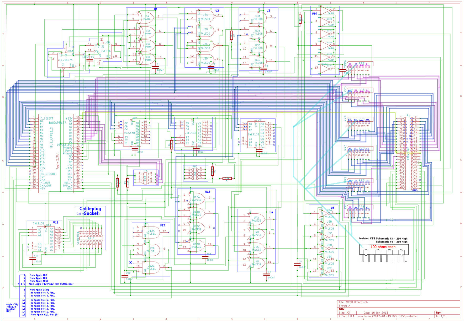
So lets first view the
origin od this signals at the IFcard - beginning from the Apple
II Slot and tracing them till to the Backpanel connector,
where they are passed along to the box: nearly all lines just pass
along through from the Apple II slotconnectionpads to the
backpanel-
connestor of te IFcard - except few lines that pass by the driver
U5 and then are passed to the connector.
 |
now lets follow up only that
traces, when they have entered the MCEB board at the connector
J1 and are passed to the "control function block" -
the picture is only a reducted part limited to the area thats related to
this lines. Recognize also the light blu enlighted line from pin
25 and 26
of J1 to the collector of the transistor Q7 ! Only if the Apple II
is powered up - this line gets + 12 Volt from the Apple II ! If
the Apple II is shut down -
Q7 can´t work.... and in such case the 2 oscillators of part 1 and part 2
won´t start oscilation and the internal part of the box won´t
have power
in that part behing the coil ( part 5 )! so this is one part of the Apple
II detection circuit ( part 8 ) besides the 4 lines mentioned
above as "special-lines".
I will return later to this page and conrinue with the
analysis.... but at the momet this explain fairly well the most
important part of the functions....
|