IBM 5150: RAM on 16KB-64KB Motherboard
4 banks of 16 KB motherboard RAM.
RAM chips of type 4116 are used, of an access time rating of 250 ns (or less, e.g. 200 ns). 4116 examples.
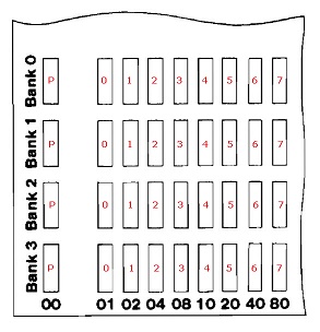
Bank 0: addresses 0 KB to 16 KB (soldered to motherboard)
Bank 1: addresses 16 KB to 32 KB (socketed)
Bank 2: addresses 32 KB to 48 KB (socketed)
Bank 3: addresses 48 KB to 64 KB (socketed)
Additional RAM can be provided by way of expansion cards, however, all four banks of motherboard RAM must be populated before RAM can be added by way of expansion cards. (Source: Note 1 on page 5-9 of the APR84 edition of the Guide To Operations manual)
The BIOS supplied with this motherboard only recognises up to 544 KB of RAM. This limitation is purely because, by design, the BIOS only reads the first 4 switches in switch block SW2.
Implications of upgrading the BIOS to the 10/27/82 one
As supplied from the factory, this motherboard was only fitted with either one of the following two BIOS revisions:
1. Dated 04/24/81. Chip U33 has "5700051" printed on it.
2. Dated 10/19/81. Chip U33 has "5700671" printed on it.
Later, IBM provided a BIOS upgrade kit for this motherboard, making the BIOS the same revision (10/27/82, "1501476" printed on U33) as found on the 64KB-256KB motherboards.
The new BIOS recognises up to 640 KB of RAM and recognises BIOS expansion ROMs.
There are two important RAM implications of using the 10/27/82 BIOS in a 16-64KB motherboard:
1. Different switch settings apply to SW2: Switch number 5 in switch block SW2 is now used. Click here to see an example.
2. Due to a bug, the 10/27/82 BIOS will almost always generate a 201 type error (e.g. "1094 201") if you do not select all 4 banks of motherboard RAM. If desired, click here for technical details about the bug.
Switch Settings
Switches 3 and 4 on switch block SW1 are set according to how many banks of RAM are populated on the motherboard (however, if you have the 10/27/82 BIOS, note the bug described earlier).
The SW2 switches are set to the total amount of RAM fitted in the 5150 (that is, motherboard + RAM expansion cards).
If you set SW2 to a LOWER amount than is fitted, there is no error - the motherboard will only recognise what was set per SW2.
If you set SW2 to a HIGHER amount than is fitted, there is a 201 memory error.
Switch settings: For the 04/24/81 and 10/19/81 BIOS, refer to pages 2-28 through 2-30 in the AUG81 edition of the Technical Reference manual.
Switch settings: For the 10/27/82 BIOS, refer to pages 5-33 through 5-50 in the APR84 edition of the Guide To Operations manual.
RAM error codes for 16KB-64KB motherboard
For a 16KB-64KB motherboard, the following error breakdown applies (irrespective of BIOS revision level).
This breakdown is slightly different to that for the 64KB-256KB motherboard.
The format of a RAM error is "bbxx 201". An example is "0510 201".
The "bb" portion of "bbxx" indicates which 4 KB block contains the faulty RAM.
The "xx" portion of "bbxx" indicates which bit in the block is the faulty one.
BLOCK INDICATOR
00xx to 03xx = Motherboard bank 0 (see 'Failure of first 16 KB bank' section below)
04xx to 07xx = Motherboard bank 1
08xx to 0Bxx = Motherboard bank 2
0Cxx to 0Fxx = Motherboard bank 3
10xx to 9Fxx = RAM on an expansion card
If required, you can calculate the failing address from the block indicator.
1. Convert block indicator from hexidecimal (hex) to decimal, e.g. 1E --> 30
2. Multiply that by 4 KB to get the address, e.g. 30 x 4 KB = 120 KB
BIT INDICATOR
XX is 00 indicates the parity chip
XX is 01 indicates the bit 0 chip
XX is 02 indicates the bit 1 chip
XX is 04 indicates the bit 2 chip
XX is 08 indicates the bit 3 chip
XX is 10 indicates the bit 4 chip
XX is 20 indicates the bit 5 chip
XX is 40 indicates the bit 6 chip
XX is 80 indicates the bit 7 chip
XX is something else indicates multiple bit failure, e.g. 24 (20+04) indicates failure of bits 5 and 2.
Note that this is done in hexidecimal. For example, A1 is broken down to 80+20+01 (indicating bits 7, 5 and 0).
Failure of first 16 KB bank
The first 16KB bank (the soldered in one) cannot be disabled.
The Power on Self Test (POST) component of all three possible BIOS revisions check the first 16 KB bank on power on of the motherboard. If the POST discovers that any of the chips in that bank are faulty, the POST will stop, providing no indication whatsoever (visual or audible). To you, it will appear that the motherboard is 'dead'.
One way to diagnose this particular problem is to use a suitable SuperSoft/Landmark diagnostic ROM in socket U33 (replacing the existing BIOS ROM).
4116 RAM chip
This chip requires 3 power sources: +12V, -5V, +5V
Therefore, if you have what appears to be a 'dead' 16KB-64KB motherboard, verify that the power supply is producing those three voltages.