WARNING : At the
following circuit diagrams i have marked up with light red shading the
so called
"primary side" of the supply. In this areas there are voltages up to 400
Volt present!
Such voltages are
lethal dangerous !
Never access this areas with present "live Voltage" ( i.e. supply
"powered up" ) !
Red highlighted areas may only be accessed while powersupply is
disconnected
from main powersource ( disconnected from powercord ) !
Never attempt this areas without ensuring the demanded
precautions of safty !
Only experienced Users with advanced knowledge and successfully
solved safty training
may work at this red highlighted areas !
Read red colored text with safty warnings ! Do not ignore this
warnings !
Ignoring this warnings may cause electric schock with lethal results !
At this page topics will be treated that relate to all powersupplies in
general ! In later parts there will be pages that treat specific parts
of feedback ( depending to the generic kind of feedback used ).at the
very end there is a page related to the more historic aspect of
the powersupplies and their development.....
Next i will show several different circuitplans related to powersupplies of
the Apple II and Apple /// series - here the first basic and most common one
of the standard "old" powersupply without any kind of feedback:
 |
later a powersupply became common that
had additional regulation / adjustment section with simple feedback:
In several Apple II
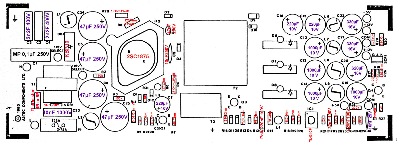
models Apple used powersupplies from the manufacturer Aztec:
That powersupply had this
layout:
Here the official version of
the Powersupply used in the Apple IIe:
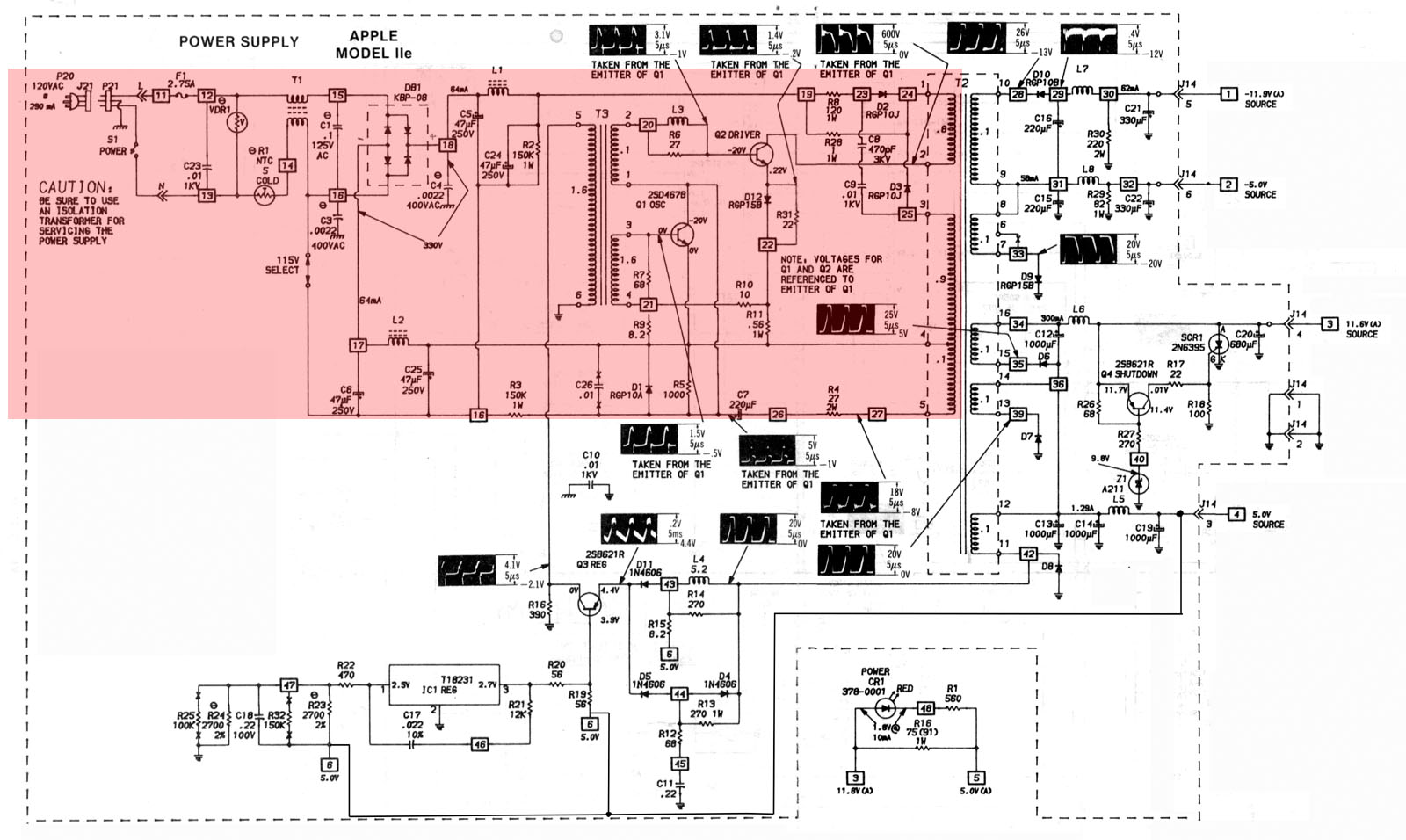
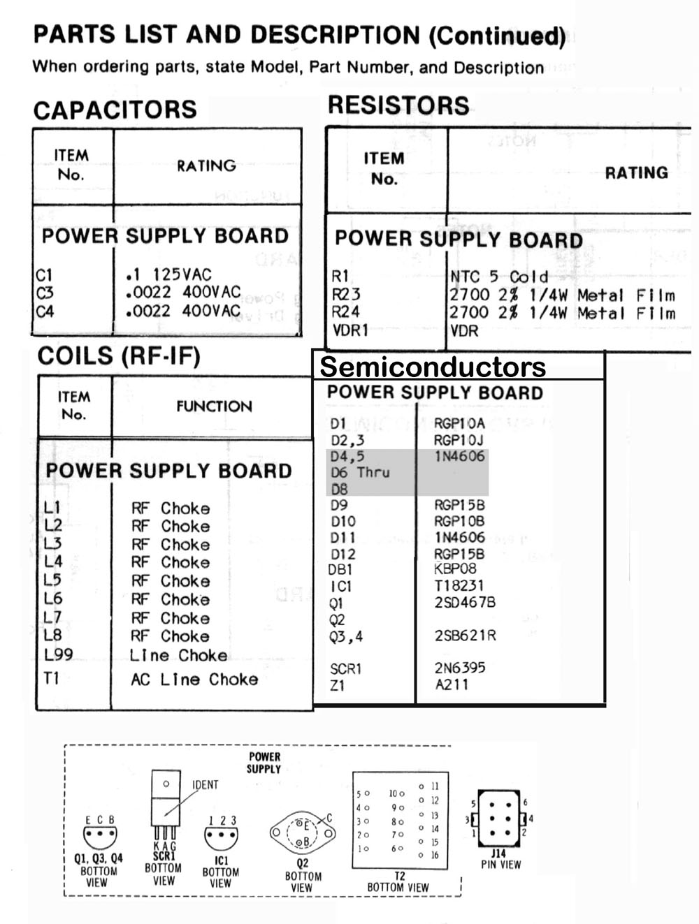
and here the partlist of that
supply:
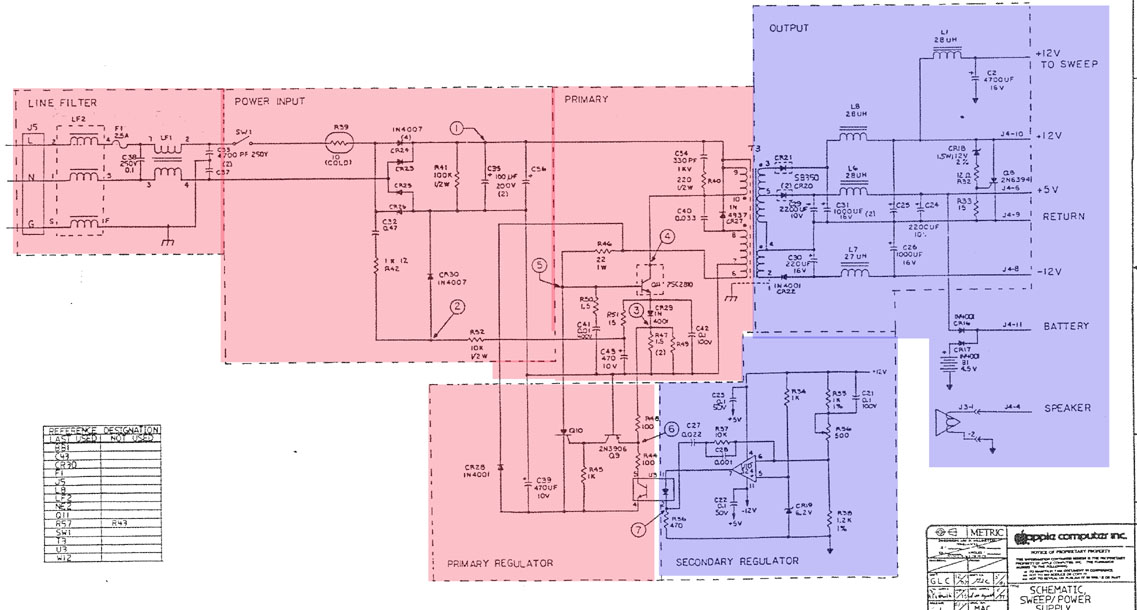
Only for few readers the next plan is
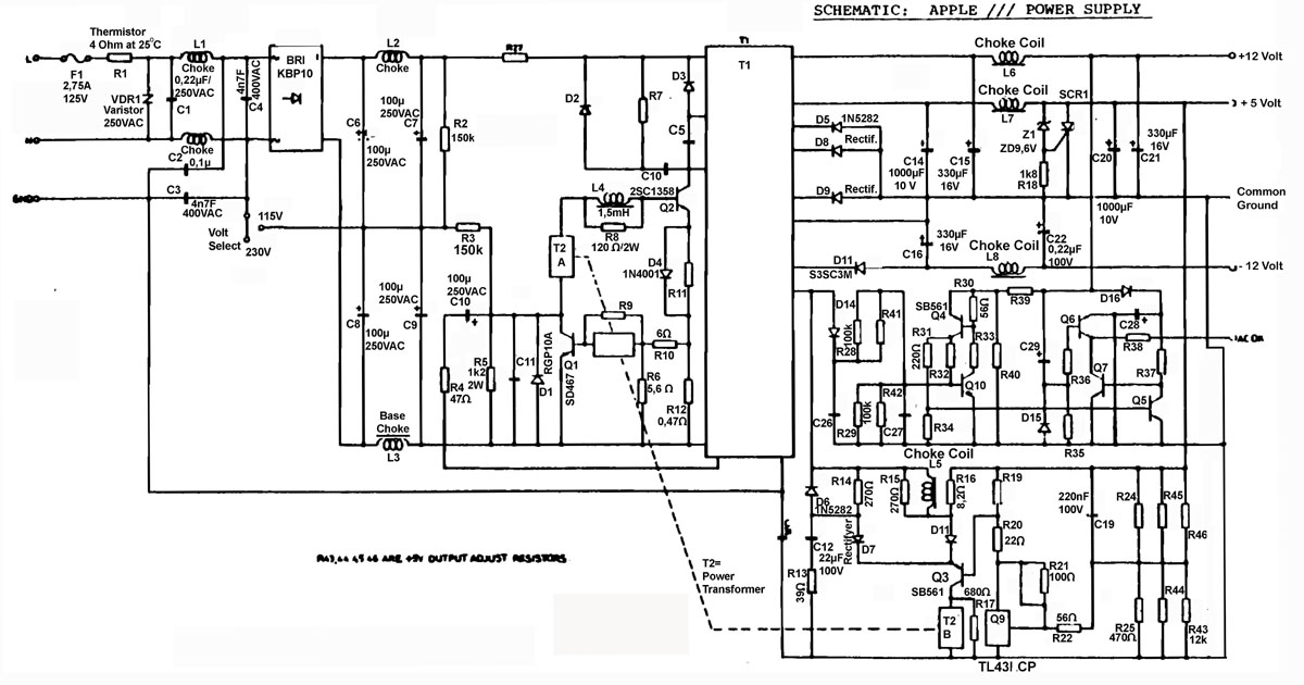
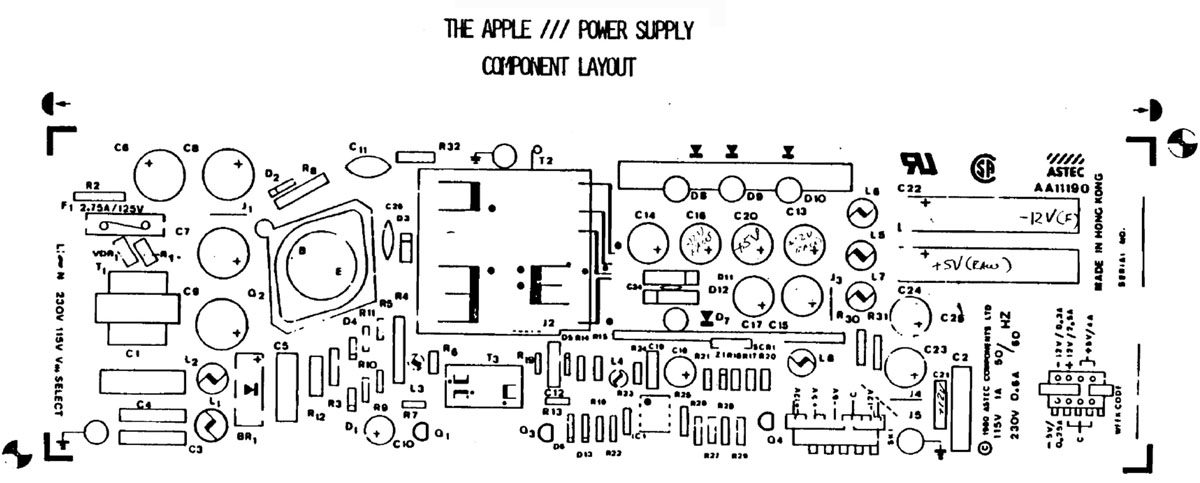
relevant - its the shematic of the Apple III powersupply:
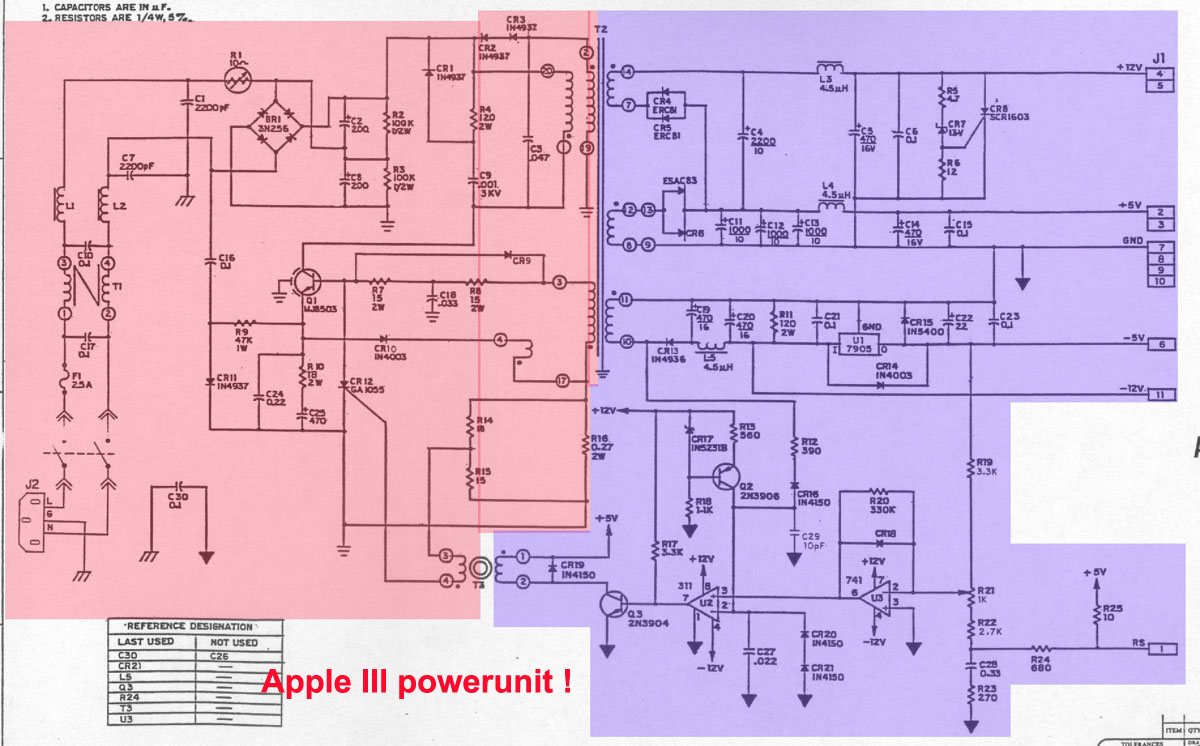
Here is the Circuitplan of a earlier Apple ///
powersupply:
the layout of the PCB looked something like this:
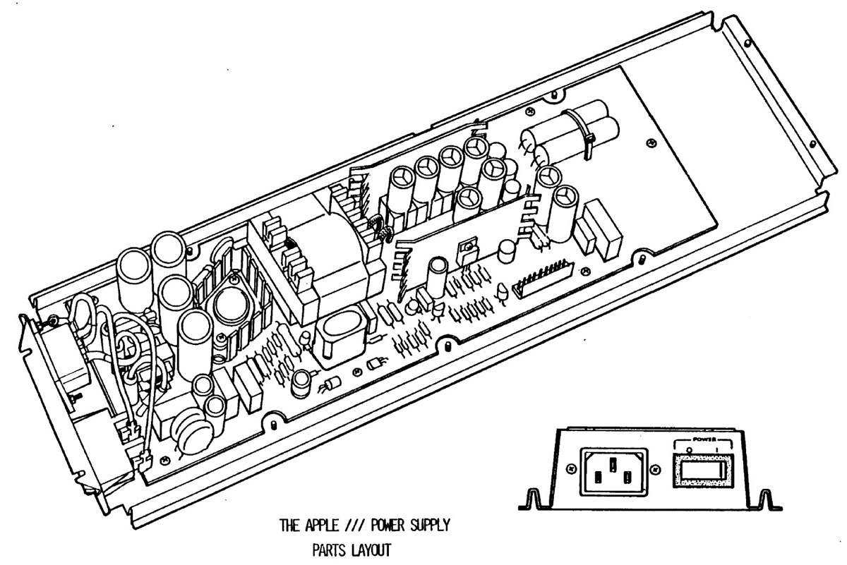
In general the view to
the Apple /// powersupply offered something like this:
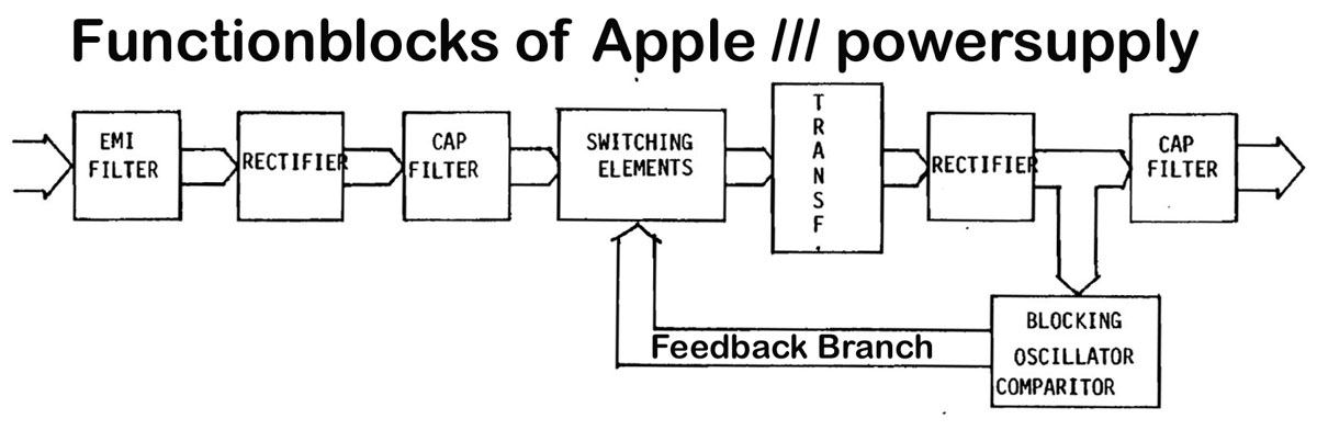
The general analysis displays the functionblocks with
this structure:
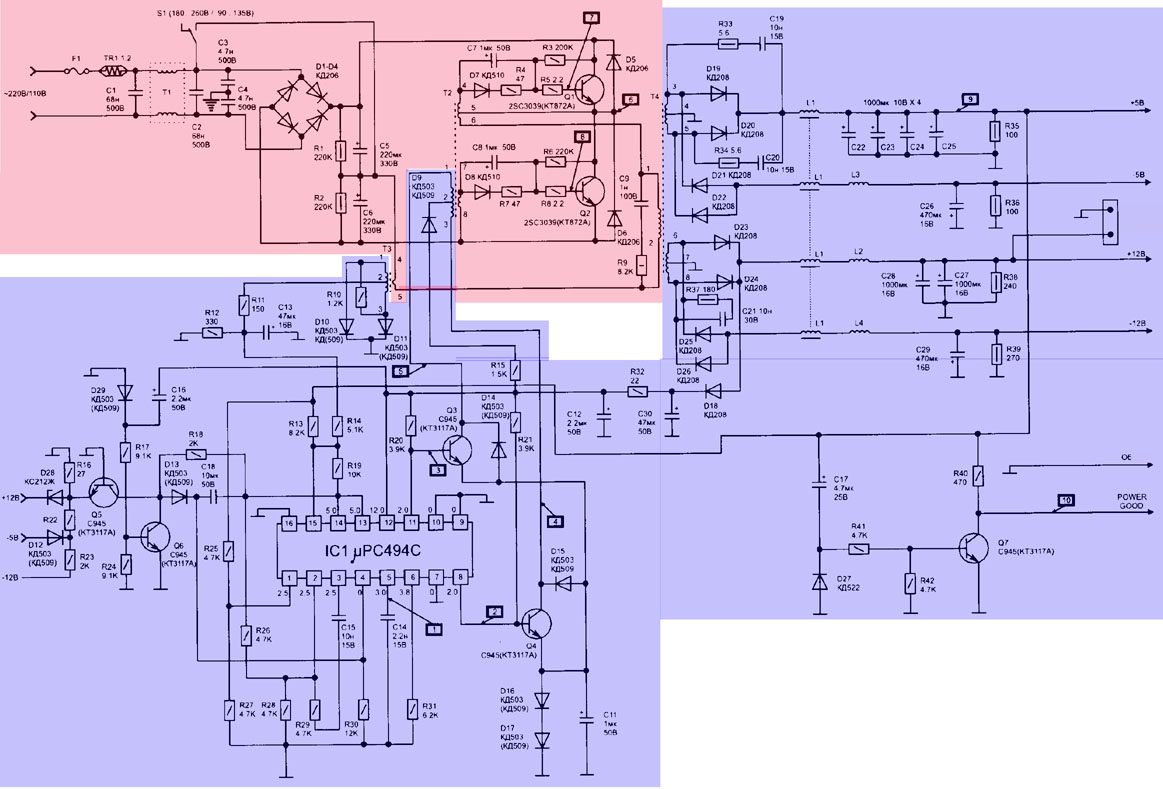
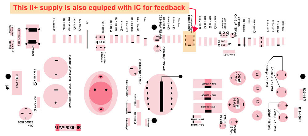
and finally here is an example of a
powersupply from 3rd party manufacturer also found in same or similar
kind at some Apple II computers with advanced feedback circuit:
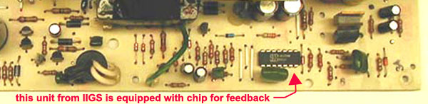
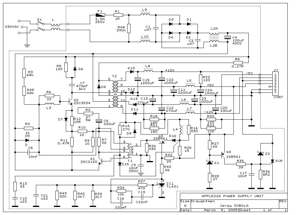
And here a Schematic of a IIGS
Powersupply:
Now let's first of all inspect some
detailed pictures of different powersupplies to learn how to sort out
which kind of supply
is related to which kind of shematic:
First a detail picture of a powersupply without feedback branch like
shown in first shematic:
Now a picture of a powersupply with
a feedback branch like related to the second shematic:
and now a detail picture of a early
IIGS supply also containing a feedback branch more similar to
schematic of third party supply:
Just to simplify the topic at the
moment:
It's rather more easy to handle the functions by using a sketch of the
function blocks instead working at the moment with the real
circuitplans. We'll turn back later to the circuitplans when discussing
details of the different variations. At the moment i just display the
circuitplans
here to enable the user to understand what is the primary section of the
power supply with dangerous voltages and what part is secondary part of
the powerunit with low voltages. In the cirsuitplans above the
dangerous primary voltage sections are marked by light red shading while
the
secondary section is shaded in light blue.
Here a view to the more simple display as function sections:
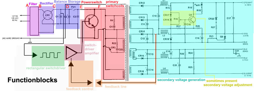 |
In the first stage the voltage passes
the Filter. The filter is a block of capacitors and coils with the
pupose to block high voltage spikes and
pulses which are every day present in the regular voltage coming out of
the wall. There are dozends of reasons for such spikes: Machines
being switched on or off, lightning strikes in the wires at far distance
away, electric power plants and connection points of that plants
switching
bypasses on or off, even a neighbor using a powerdrilling machine will
cause spikes in the voltage within the house or even at the house next
door.... the filter is targeting only for this very short pulses of few
milliseconds and keeping them away from the following circuits.
The next stage is the rectifier. Classic rectifiers can be made in
different ways.... in the specific use at switching power supplies here
in general so called bridge rectifiers are used. In some rare cases such
bridge rectifiers are replaced by a construction of 4 diodes.
General simple statement will be: at 2 pins AC voltage is put in the
bridge and at the remaining pins at one pin is a positive and at the
other
pin there is a negative voltage so after the rectifier is only DC
voltage present - allthough this voltage is still not stable and still
flowing with
with variable peak.
This is the reason for the next functionblock the "balance storage". It
consists of large capacity electrolytic capacitors. While voltage peak
is
lower it unloads voltage while in high peak it collects power and stores
it for short period of time till peak drops below storage voltage and
power to outout is passed out from that stored power. So before this
function block the avarage peak to peak is about difference of 35 %
at the output that voltage is "equalized" to peak to peak less than 5%
difference.
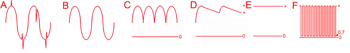 |
The stripe above displays symbolic the
waveforms that you may see with an oscilloscope at the functionblocks
above at the same marked
letters. After the AC voltage A has been
cleaned from spikes at B and rectified at
C and egalized at D
the "clean" DC voltage at E is
directed to the switching power transistor and that powertransistor
switches the voltage F between the
availiable high potential and
0,7 Volt in squarewave form which is then injected to the transformer.
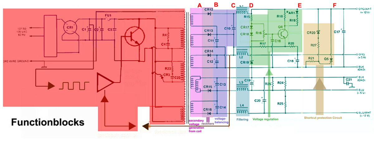
In the next function block shematic we'll skip from the primary voltage
section to the secondary voltage section. In general it has similar
function blocks due to the fact the at the primary side of the
transformer a squarewave signal is injected and at the secondary
isolated
windings there is resulting from that a nearly also sqarewave output of
voltages at the various secondary windings too. The frequency
of that squarewaves is far higher than the turnaround frequency of the
net wall outlet. The frequency at the transformer in this power
supplies is rated between 50.000 Hz ( 50 kHz ) and 120.000 Hz (120 kHz )
depending from model and typ of switchfrequency generation.
That squarewaves are then rectified with simple high current switching
diodes in the rectifier section and gathered in each voltagebranch
at the large electrolytic capacitors that act as a voltage balancing
unit by collecting voltage while loading at high peak level and passing
the collected voltage while voltage drops at input to less higher peak
level and thereby "equalizing" the output voltage. Due to the fact
that there is still a high portion of remaining high frequency swing at
this voltage in the next step the voltage passes a high potential
blocking filter coil that filters off that high frequency portion and at
that output then nearly pure DC Voltage.
Depending to the kind of powersupply used, some of that powersupplies
then are equipped with a system of voltage regulation /
adjustment that is related only to secondary power control. In some
other systems this regulation is coupled to the primary side
by use off an isolating optocoupling device / chip and "feedback"
techniques.
And in some devices there is a rather simple secondary "shortcut
protection" circuit - while at some other devices there is a more
difficult
"shortcut protection circuit" taking influence to shut off the primary
part of the power supply ( also by using a kind of "feedback"
technique.
In this case at the circuitplan below ( which is equal to the
powersuplly used by Apple itself in the silver aluminium power supply
cases.
Unfortunaty i don't have any supply from that ancient kind of series.
But at applefritter thankfully a member "fri0701" made a lot of usefull
pictures to that kind of powersupply and mailed them to me, enabling me
later to explain details of that supply with his pictures.
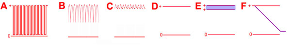
 |
Like in the primary part of the
powersupply in the previous explenation also here at this point i have
made a sketch of the kind of
wavetypes and voltagedisplays that will be seen at a measurement by
oscilloscope in such supply above at the points marked
by A till F
corresponding to the points marked in the path of the circuitplan above.
Please also recognize the orientation of
the Diodes ( CR12 to Cr15 ) in different voltage paths at the stage
of rectifiers.
The orientation of the diodes is responsible for the fact, if
that branch later provides the line with positive or negative voltage
!
E marks a varibable area within the voltage may be adjusted ( +/-
10% )
and the sketch of F marks by the violet
line the shutdown and limiting of the current and outputvoltage - if the
shortcut protection
circuit is triggered and becomes active.
| |
 |
In later sections of the text the very
specific other variations of voltage adjustment and feedback
regulations will be treated. At the
moment we will stay focused to the basic and general functions of the
powersupply that are present at every of this
power supplies.
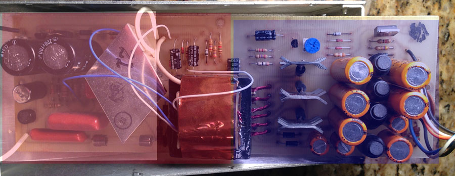
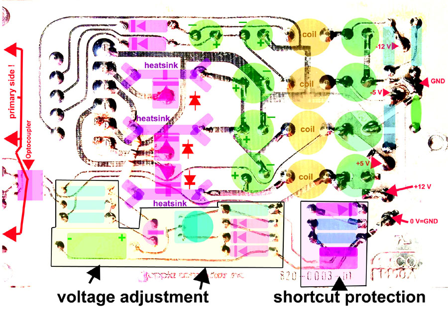
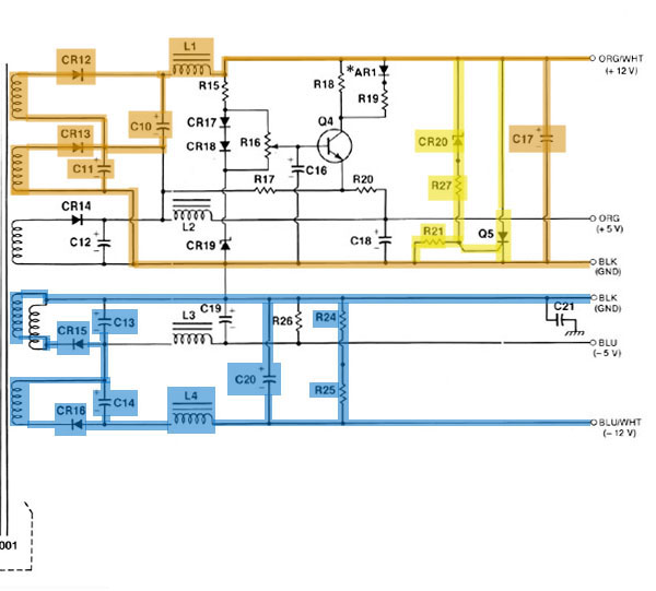
Now let's compare circuitplan with "real" PCB from powersupply in silver
aluminium case - first splitting dangerous primary section
( shaded in light red ) from secondary section ( shaded in light blue )
appart:
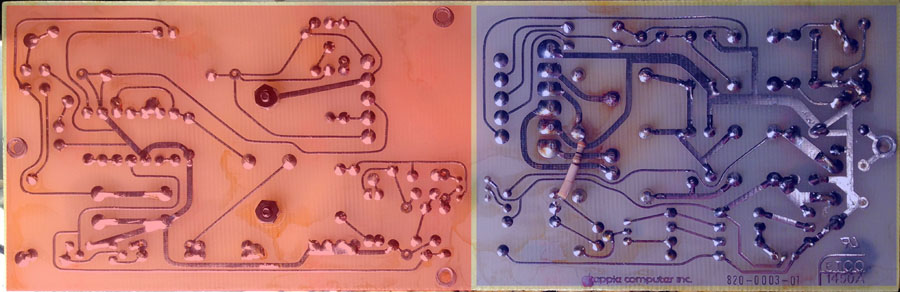
from top:
from soldering side:
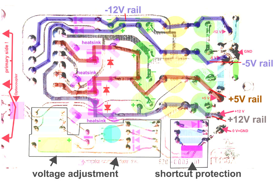
next we will take a view back to the
secondary section at the circuitplan and just mark up the voltage paths
splitted apart:
here the section related to the + 12 Volt and -12 Volt path:
- and here the sections related to the +5 Volt and - 5 Volt path:
 |
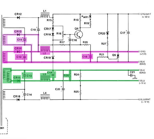 |
Recognize the
shortcut protection circuit marked by light yellow shade !
It's connected to the + 12 Volt rail !
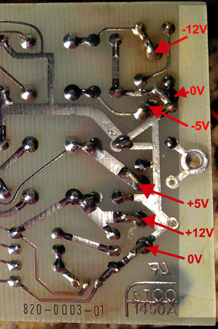
And in picture below the
GND=0 Volt Trace is marked at soldering side of PCB with red
color :
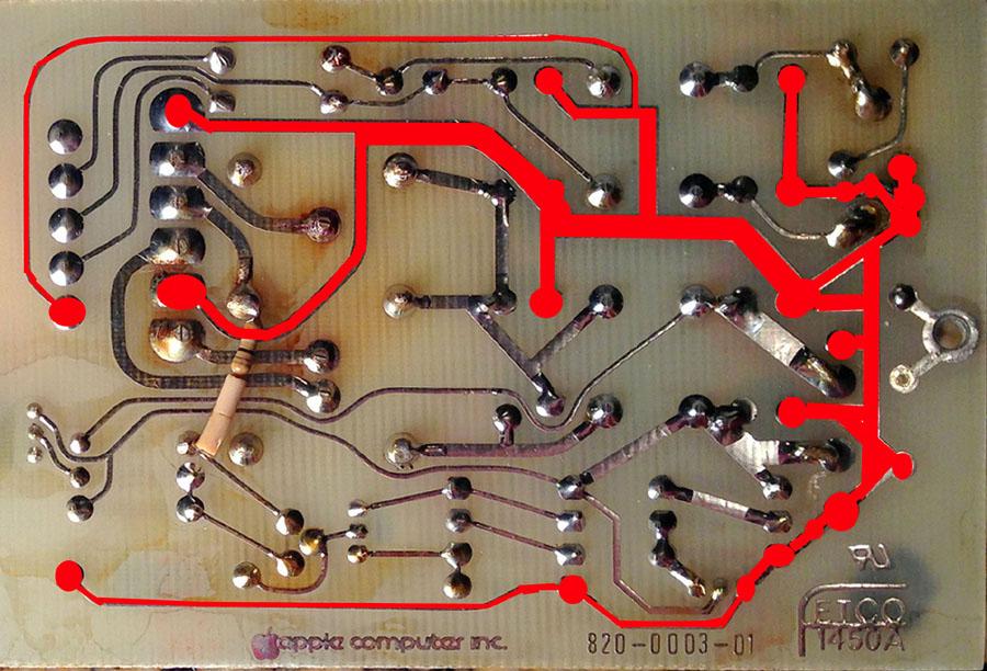 |
And in this
pictures the soldering points of the ouput voltages
marked at topview and from solderside:
|
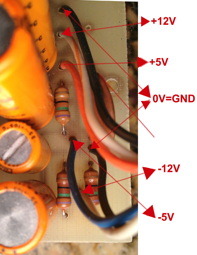
And now the allocation of the
different voltage rails related to the view at solderside and at
componentside:
Note that at the transformer the
+ 5 Volt rail starts first at 2 different coiloutputs from the
transformer and later both rails are joined together at the
electrolytic capacitors and the
common final part of the + 5 Volt rail is then along the one
filter coil and the final
loading electrolytic capacitor. This is related to the fact that
at the output of the transformer 2 windings are used to collect
the high current ( each path 2,5 Ampere ) and
rectify them before then the voltage ( total of 5 Ampere ) is
leading to the filter coil filtering
the current of both rails.
Also note that the large rectifying diodes in the positiv
voltage branches ( all 3 mounted to
cooling sinks ) are connected that way, that the Anode is
connested to PCB while the Kathode is soldered to the heatsink
and the
soldering of the heatsink to the PCB leads the voltage to
the following electrolytic capacitors ! |
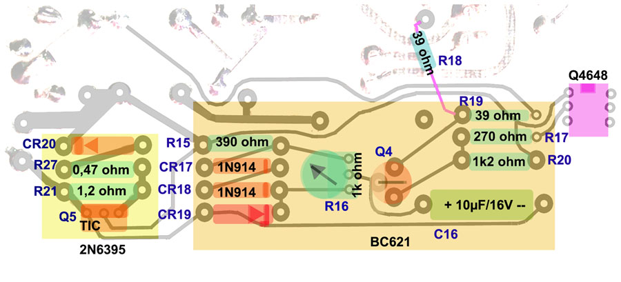
|
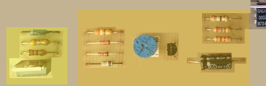
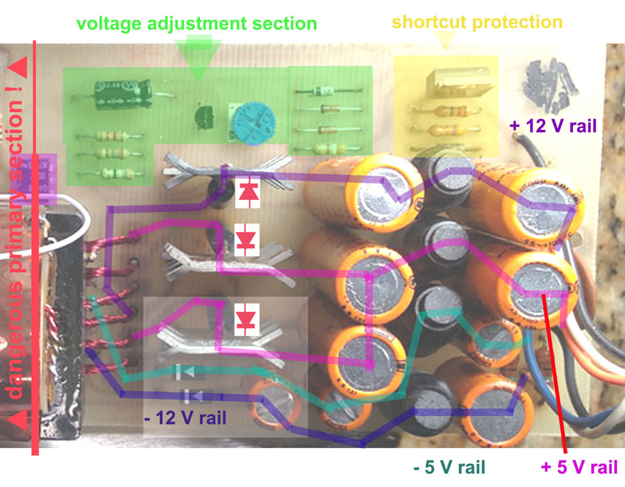
Now at this point we'll take a closer
view to the components of the shortcutprotection and the the
voltageadjustment and allocate the components
in real PCB to the components in the circuitplan (
for better view the PCB has been turned 180 degrees ! ) :
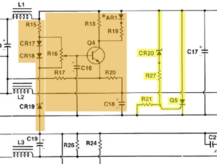
Note:
The powersupplies have slight variations at the use of
components.
Therefor i'm still collecting some of the used components that
have been
dependent to availiability - among
the components there was slight
differences with CR20 ( the
Trigger- Diode used for shortcut
protection ),
Q5 ( the Triac in the
schortcut protection ), CR 19 ( the
reference zener-
diode in the voltage adjustment and the used
transistor Q4.
The diode AR1 often was not used,
but instead a wire bridging that place. |
|
And here some detail explenations
about the so called "shortcut protection"
( marked above with yellow shading ):
In fact the shortcut protection is a circuit that makes another shortcut
! Under normal operating conditions the current and voltage
running along the 12 Volt rail limits the voltage and current running
along the path from CR20 R27 and
R21 and the result will be,
that at the junction of R27 and
R21 the voltage is to low to trigger the
Triac Q5. In that condition the triac
Q5 remains blocking
and the voltage and currrent can proceed to the output cable and
outputplug of the supply. If a damage happens in later
stages behind the powersupply this will cause the voltage and current
running along the path CR20, R27 and
R21 to change
and at the junction of R27 and
R21 the voltage above
R21 will raise and then inject the voltage requested to trigger
the triac Q5
to open and the entire voltage and current is passing through the triac
Q5 to GND like if there would be a shortcut. This then
thereby prevents the voltage and current to continue it's path to the
output cords and plug to the mainboard of the computer.
By this "trick" the voltage is kept off from the mainboard
till the regular fuse at the primary input is
melted down and tears off
the voltage from the primary section of the powersupply and the unit is
"switched off".
The reason for this kind of "trick" is the speed
of reaction: That fuse at the primary section is (
by terms of electronics ) rather slow
*)
( it takes at least about 15 milliseconds
to melt that fuse wire in the primary section ) - while the circuit at
the shortcut protection rail
is able to "switch away" the voltage from mainboard within only about 25
nanoseconds !
*) [ 15 milliseconds =
0,015 seconds <= /
/ => 25 nanoseconds = 0,000025 seconds
! ]
But this "trick" has some points of "weakness":
While the shortcut is switched at the Q5 -
this device can get really hot ! This might cause that device to become
damaged internal
without visible signs at the outer casing ! Specially because ( probably
for reason of cost saving ) this Q5 is not
equipped even with
simple smallest possible cooling sink !
In some cases the triggering zenerdiode CR19
can get damaged by heat too and then remains in a state permanently
trigerring the
Q5 even if there is no shortcut anymore
because the damage at the mainboard has been solved.....
So a general rule is:
If you are sure, that at the
voltageoutput plug of the powersupply there is for
sure no more shortcut present
and the powersupply itself still refuses to pass the voltages to the
plug and you still hear a kind of "chirping noise" caused by a
permanent switching of this shortcut protection - then it's highly
recommended to replace the CR19 zenerdiode
by a exactly same
new one and replace the Triac Q5 also
exactly with same new device ! It is
strictly recommended NOT to use similar kind of device !
The reason for this: Different kinds of
zenerdiodes have slight minor differences in
behaviour at various temperatures and same is valid
to the triacs - they also have by small differences (
see datasheets of the device in any case of doubt
! ) in behaviour like small
changes in triggering voltage and behaviour at different
temperatures ! The resistors at the path R27
and R21 following the
CR19 are
exactly calculated by math to
split the voltages in the path to the
different junctionpoints of that path ! If you use other "similar"
but not exactly same components you must
bear in mind that this will require recalculation
of that resistors to ensure correct
voltage values during normal operation mode and ensuring that in case of
mistakes at the mainboard the voltage at the junctionploint
of R27 and R21
really reach the limit required to cause the Q5
triac to be triggered !
Note at this point:
There are also several other methods of shortcut
protection used by other powersupplies which are related
to more complex circuits ( in general with use of
"feedback" to the primary section of the powersupply ...... ) -
this kind of protection
will be explained at later point of this pages while explaining "feedback"
and various kinds of "feedback" techniques and various
purposes of "feedback".
So next we will take
a closer view to the "voltage adjustment".
In this specific case we will only examine the
voltage adjustment at the secondary section. The other kind of
voltage adjustment by "feedback"
technique will be examined in later part of the pages. Lets take a
closer view to the circuitplan above and the light brown shaded area.
the first part of the voltage adjustment is realized by the path of the
resistor R15, the 2 diodes
1N914 and then the zenerdiode
CR19.
The resistor limits the current running along the path to several
milliamperes and then the voltage passes the 2 diodes
1N914 by
decreasing the voltage below each of the diodes by
0,7 Volts and after passing the 2 diodes (
CR18 and CR17 ) the voltage is
limited to
the "breakthrough" voltage of the zenerdiode
CR19. In general use the zenerdiode CR19
therefor will be a typ of ZPD 10 Volt or
ZPD 9,1 Volt.
So in this case the measured voltages will be: At the Junctionpoint
between CR19 and CR18
depending to the used zenerdiode
the voltage limited by the zenerdiode itself - either
10 Volt or 9,1 Volt.
At the Junctionpoint between CR18 and
CR 17 either 10,7
Volt
or 9,8 Volt resulting to a voltage
0,7 Volt above of the limited voltage at
the zenerdiode and at the junctionpoint between
CR17 and
the resistor R15 the voltage will be at
either 11,4 Volt or
10,5 Volt ! So at the both ends of the regulating trimming
resistor R16 there will be
either 10 Volt and
11,4 Volt present or in the other case there will be the voltages
9,1 Volt and 10,5
Volt present ( depending to the used
zenerdiode CR19 ! By the path the user may
be able to adjust the voltage at the junctionpoint between
R16,the electrolytic capacitor
C16
and the transistor Q4 a voltage between
this to limiting values explained in previous sentences..... ( either
10 Volt to 11,4
Volt
or 9,1 Volt to 10,5
Volt ). The purpose of the electrolytic capacitor is to keep the
voltage in smooth stability ( with out pumping up and
down ) and stabilizing the voltage at the base
connection ot the transistor Q4.
The real "regulation path" is realized by the 2 resistors
R18 and R19 in
the upper part of the trail, the "inner resistance"
of the transistor Q4,
and the resistor R20 at the lower end,
which is connected to the 5 Volt rail at the junctionpoint
R20 and the electrolytic capacitor
C18.
The transistor might be viewed in this path as a kind of "electronic
controlled variable resistor" that is controlled by the voltage
at
the base connection of the transistor. If a
lot of current and voltage is at the base
the transistor will open the path between emitter
and collector ( the 2
outer pins ot the transistor ) and act like a "smaller
resistor" - while if the power is taken away from the
base
of the transistor it will shutdown the path between the
emitter and collector
( the 2 outer pins of the transistor
) and act like a
"larger resistor with higher resistance"
and blocking the path from +12 Volt to + 5 Volt.
So "opening up" the transistor by turning the
trimming resistor pin towards the junctionpoint at
CR17 and R15 will "pull up" the
voltage from 5 Volt towards the + 12 Volt resulting
to the 5 Volt rail being "pulled up" towards 5,6
Volt - while turning the pin of the resistor
R16 towards the junction point at
CR18 and
CR19 will close the path between +12 Volt
and the 5 Volt rail resulting the 5 Volt rail to
drop down towards 4,8 Volt.
Note in case of
malfunction:
If the voltage adjustment fails ( resulting to missing ability to
regulate the voltage within a specific range ) there are 5 more possible
reasons - assuming that there are no visible damages at the resistors
like brown shades resulting from inner high temperature or burn
of the resistor.
The highest risk to fail will be the zenerresistor
CR19 - it get's damaged if the current passing through the device
exceeds
the limits of the component. In some PCB's there are still typ's used
that only permit maximum of 100 milliampere. In later PCB's there
often was used a stronger typ the permits a limit of 500 milliampere.
The visible difference is that the weaker version
has a glass casing
while the stronger typ is cased in plastic.
The next chance to fail will be the transistor Q4.
Often in that old PCB's there were transistors used with very limited
ability of "power
consumption" ( 150 milliwatt ) resulting to the fact that such a
transistor can "age by higher temperature" caused by stronger current
running along the path from emitter to collector. In later PCB's
stronger transistors with higher ability of "power-consumption" ( up to
500 milliwatt ) have been used ( consult the datasheet of the used
transistor in case of doubt ). Such stronger transistors had less
tendency to fail. In case of replacement therefor it might be a good
idea to use as replacement typ a stronger replacement typ instead
of the former used one - but such "upgrade" should be performed by
experienced technician who is able to judge by datasheet data,
if the replacement transistor will execute correct it's duty.
The final chance for mistake will be a damage of both diodes 1N914
CR18 and CR17.
If they are damaged there will be no difference of
voltage ( which is by the definition of the diodes 1,4 Volts ! ) between
the junction at CR19 and CR18 and the
other junction
at CR17 and R15. If
there is no difference in the voltage, there is no adjustment range
! In such case both diodes should be replaced.
So at the next page i will start with more specific topics related to
the "feedback" variations.
|