| Home |
Step
| Action
| Comment
| Reference
|
1 |
8088 PROCESSOR TEST |
If the test fails, halt the CPU. |
Page 5-34 |
2 |
DISABLE NON MASKABLE INTERRUPTS |
Disable NMIs from reaching the CPU. |
Page 5-35 (line 370) |
3 |
DMA CHAN 1 PAGE REGISTER |
Zero the page register for DMA channel 1. |
Page 5-35 (line 371) |
4 |
DISABLE VIDEO |
Page 5-35 (lines 372-376) |
|
5 |
8255 OPERATION |
8255 PPI chip. Set port B lines to outputs. See note 11 for more info. |
Page 5-35 (lines 377-378) |
6 |
8255 OUTPUTS |
Set the 8255's port B lines to various states. |
Page 5-35 (lines 379-380) |
7 |
ROS CHECKSUM TEST I |
Verify that the checksum of the BIOS ROM, U33, is 00. If verification fails, halt the CPU. (U33 = 8 KB block at FE000) |
Page 5-35 (lines 381-380) |
8 |
TEST TIMER 1 |
Timer #1 on 8253 interval timer chip. Used in RAM refresh process. If the test fails, halt the CPU. |
Page 5-35 (lines 402-430) |
9 |
INITIALIZE TIMER 1 |
Initialise timer #1 with divisor of 18 - results in one pulse per approx. 15 µs. |
Page 5-35 (lines 435-436) |
10 |
8237 DMA TEST |
Test 8237 DMA controller chip. If the test fails, halt the CPU. |
Page 5-36 (lines 439-462) |
11 |
START RAM REFRESH |
Initialise and start DMA for RAM refresh (RAM refresh done via dummy DMA transfers). |
Page 5-36 (lines 464-486) |
12 |
EXPANSION I/O BOX - ENABLE |
Write 1 to port 213h. If an extender card for the IBM 5161 Expansion Unit is present in the 5150, that action enables the extender card to communicate with the 5161. Presumably, this enabling is done now so that any RAM in the 5161 is zeroed in step 15. See note 6 for more information. Page 5-36 (lines 498-500) | |
13 |
BASE 16 KB RAM TEST |
If a cold boot, test the first 16 KB of RAM. If the test fails, halt the CPU. |
Page 5-36 (lines 502-508) |
14 |
ZERO MOTHERBOARD RAM UP TO 64 KB |
Size determined by examination of switches 3/4 on switch block SW1. Assumes that RAM banks on motherboard are 16 KB sized. See note 7. Done on both cold and warm boots. For cold boots, the act of writing to each RAM address will appropriately set/reset the parity bit of each address. See note 5. |
Page 5-36 (lines 509-520) |
15 |
ZERO RAM PAST 64 KB |
Upper limit of RAM determined by examination of switches 1 to 5 on switch block SW2. See note 8. Done on both cold and warm boots. For cold boots, the act of writing to each RAM address will appropriately set/reset the parity bit of each address. See note 5. This code contains a bug. See note 10. |
Page 5-37 (lines 525-551) |
16 |
8259 INITIALISATION |
Initialise the 8259 interrupt controller chip. |
Page 5-37 |
17 |
8259 TEST |
If the test fails, beep 1 long then 1 short, then halt the CPU. |
Page 5-38 |
18 |
TEST/SET TIMER 0 |
Timer #0 on 8253 interval timer chip. If the test fails, beep 1 long then 1 short, then halt the CPU. |
Page 5-38 |
19 |
INIT/START VIDEO CONTROLLER |
1. Initialise monochrome and CGA video cards. On failure, beep 1 long then 2 short. (Because of a bug, 1 long then 2 short can also occur in step 26.) 2. Look for BIOS expansion ROMs in address block C0000 - C7FFF. Those will be video ROMs in EGA/PGA/VGA cards. If one found (first 2 bytes are 55/AA), verify that its checksum is 00, and if that verification passes, call the initialisation code in the ROM. If the verification fails, then display the segment address of faulty ROM followed by "ROM" (e.g. "C000 ROM"). See note 4 for more information. |
Page 5-39 |
20 |
EXPANSION I/O BOX - TEST |
If an extender card for the IBM 5161 Expansion Unit is fitted in the 5150, then test communications with the 5161. If the test fails, display an "1801" error. |
Page 5-41 |
21 |
CALCULATE TOTAL RAM |
Calculate the total RAM. This code contains a bug. See note 9. |
Page 5-42 (lines 934-951) |
22 |
ADDITIONAL RAM TEST |
If a cold boot, test the RAM past 16 KB. If the test fails, display the number (in hex) of the failing 4 KB block followed by bit error pattern, followed by " 201". Example: "0510 201". Click here for detailed information. |
Page 5-42 (lines 952-998) |
23 |
KEYBOARD TEST |
If the test fails, display a "301" error. See note 13 for possible causes. |
Page 5-43 |
24 |
INTERRUPT VECTORS |
Set up the interrupt vector table. |
Page 5-43 (lines 1034-1049) |
25 |
CASSETTE PORT WRAP TEST |
If the test fails, display a "131" error. During this test, expect to see the insides of the relay (K1, next to cassette connector) move, accompanied by a low-level click sound. See note 12 for possible causes. |
Page 5-44 |
26 |
EXPANSION ROM SEARCH |
Look for BIOS expansion ROMs in address block C8000 - F5FFF (see note 3). For each one found (first 2 bytes are 55/AA), verify that its checksum is 00. If verification passes, call the initialisation code in the ROM. If verification fails, then display the segment address of faulty ROM followed by " ROM" (e.g. "D000 ROM"). BUG: Because of a bug, if the faulty ROM starts at C8000 (which is the norm for an XT class hard disk controller), instead of "C800 ROM" being displayed, there will be 1 long beep then 2 short beeps. See note 2 for more information. |
Page 5-44 See note 1 for more info. |
27 |
ROS CHECKSUM TEST II |
Verify that the checksum of each of the four BASIC ROMs (U29/U30/U31/U32) is 00. On failure, display segment address of faulty ROM followed by " ROM" (i.e. "F600 ROM" or "F800 ROM" or "FA00 ROM" or "FC00 ROM"). |
Page 5-44 |
28 |
DISKETTE ATTACHMENT TEST |
Only performed if switch 1 on switch block SW1 is in the OFF position. Test communication with floppy controller card. On failure, display a "601" error. Via controller, turn floppy drive A: motor on. Via controller, move heads of floppy drive A: to track 1. On failure, display a "601" error. Via controller, move heads of floppy drive A: to track 34. On failure, display a "601" error. See note 14. Via controller, turn floppy drive A: motor off. |
Page 5-45 |
29 |
SET UP KEYBOARD BUFFER |
Page 5-45 (lines 1188-1194) |
|
30 |
8259 - ENABLE TIMER/KYB INT |
Enable interrupts from 8253 timer [chan. 0] and keyboard. |
Page 5-45 (lines 1195-1197) |
31 |
DETERMINE LPT (PARALLEL) PORTS |
Page 5-45 (lines 1198-1216) |
|
32 |
DETERMINE COM (SERIAL) PORTS |
RS232 |
Page 5-45 (lines 1217-1241) |
33 |
GAME CARD |
Is a game card present? |
Page 5-46 (lines 1242-1246) |
34 |
SET LPT/COM TIMEOUTS |
Page 5-46 (lines 1249-1259) |
|
35 |
ENABLE NON MASKABLE INTERRUPTS |
Page 5-46 (lines 1263-1264) |
|
36 |
BEEP 1 SHORT TONE |
Page 5-46 (lines 1267-1268) |
|
37 |
DO BOOTSTRAP |
Attempt to boot from A: (if switch 1 on SW1 is OFF), else try C: (if present), else run cassette BASIC. |
Page 5-46 (line 1271) |
| Note 1 | Page 5-44: ROM_SCAN - The code that does the search. Page 5-48: ROM_CHECK - The code called to see if a particular ROM has an expected checksum of 00. Page 5-53: ROM_ERR - The code called if a ROM's checksum is bad (not 00). |
| Note 2 | The bug is in routine ROM_ERR (page 5-53 of reference). One of the things this routine does is determine if the bad ROM (checksum not 00) is either: 1. A video ROM; or 2. Some other type of BIOS expansion ROM. It does that by examination of DS. If DS is less than C800, a video ROM is indicated. The bug is that "JLE ROM_ERR_BEEP" has been used instead of "JL ROM_ERR_BEEP". Bug verified using a simulated corrupt ROM (EPROM with tenth byte altered) in an NDC5127 MFM controller. The bug has been corrected in the 5160 BIOS |
| Note 3 | Start signature of ROM checked for in 2 KB increments: C8000, C8800, C9000, --> F5800 The last address checked is F5800, which makes sense because the 10/27/82 BIOS starts at F6000. Block end address incorrectly commented as "F4000" in source code. It should be "F6000". |
| Note 4 | The initialisation code in some video ROMS produce their own error beeps. Example: IBM EGA cards produce 1 long beep followed by 3 short beeps. |
| Note 5 | On power on of the computer, the contents of motherboard RAM will be somewhat random. That means that for a certain portion of addresses, the content of the parity bit will not reflect the parity of the combined data bits. After POST completion (non maskable interrupts enabled), attempts to read from such addresses would result in a parity error. By writing (anything) to the addresses now, the parity bit at the address is appropriately set/reset. |
| Note 6 | This step may not actually be required because in the IBM documentation on the IBM 5161 is, "The expansion unit is automatically enabled upon power-up." It is reinforced by the fact that this step was not included in the 01/10/86 revision of the 5160 BIOS. |
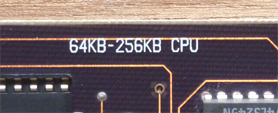
| Note 7 | Even though on the 64KB-256KB motherboard, where the RAM banks are 64 KB sized, this routine assumes that RAM banks on motherboard are 16 KB sized. If switches 3/4 set to on/on (bank 0), calculated motherboard RAM is 16 KB. If switches 3/4 set to off/on (banks 0/1), calculated motherboard RAM is 32 KB. If switches 3/4 set to on/on (banks 0/1/2), calculated motherboard RAM is 48 KB. If switches 3/4 set to off/off (banks 0/1/2/3), calculated motherboard RAM is 64 KB. |
| Note 8 | What is calculated, and stored in IO_RAM_SIZE for later use, is the KB size of RAM past 64 KB. Example: If SW2 settings are set for 256 KB, calculated for IO_RAM_SIZE is 192 KB. By "IO_RAM", IBM means RAM on expansion cards. Therefore, when this BIOS is on a 16KB-64KB motherboard, "IO_RAM" is a proper description. But when this BIOS is on a 64KB-256KB motherboard, the use of "IO_RAM" is incorrect. Instead of "IO_RAM_SIZE", IBM should have used something like "RAM_PAST_64K". |
| Note 9 | The bug only presents a problem if less than 4 banks of motherboard RAM are populated. For more information, read the BUG #1 section in 5150_27OCT82_less_than_4_ram_banks.htm |
| Note 10 | The bug only presents a problem if less than 4 banks of motherboard RAM are populated. For more information, read the BUG #2 section in 5150_27OCT82_less_than_4_ram_banks.htm |
| Note 11 | At power on (and after RESET released), the 8255 defaults to mode 0 operation for both groups, with all 3 ports (A, B and C) being inputs. So, even though the command sent to the 8255 is [Group_A_mode=0, Group_B_mode=0, Port_A=inputs, Port_B=outputs, Port_C_upper=inputs, Port_C_lower=inputs], the only result is that the port B lines change from inputs to outputs. |
| Note 12 | Some (not all) known causes: 1. Motherboard of type 64KB-256KB is not receiving minus 5 volts. Try reseating plug P9 from power supply, in case of bad connection. 2. Motherboard relay K1 is 'stuck'. |
| Note 13 | Some (not all) known causes: 1. AT class keyboard attached. That will not work. A PC/XT class keyboard is required. 2. Keyboard accidentally attached to cassette connector instead of keyboard connector. 3. No keyboard attached. 4. Faulty keyboard. |
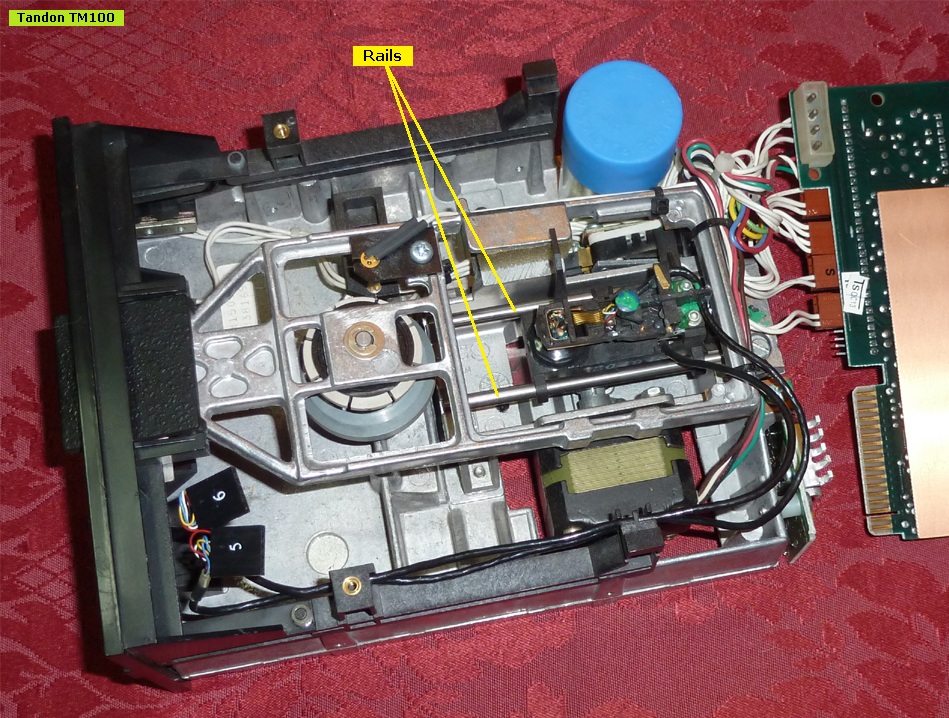
| Note 14 | The only form of head position feedback that the floppy drive electronics has, is a switch that detects whether or not the heads are at the first track. And so the drive really doesn't know if the heads got as far as track 34. For example, deteriorated lubrication on the drive's rails (resulting in intermittent head stepping) may mean that the heads only got as far as say, track 22. In that example, the drive is faulty (intermittent head stepping), but the 601 test is passing because the drive is unable to detect exact head position (except for the heads being on the first track). |