Home

IBM 5150  -  Motherboard Switch Settings


SW1 and SW2 are the two switch blocks on an IBM 5150 motherboard.


On versus off

For switches, some people are unsure about which position is on and which position is off.
If you are unsure, then click here to see examples.


Switch block SW1

Of SW1 and SW2, SW1 is the switch block closest to the center of the motherboard.
These settings apply to both the '16KB-64KB' and '64KB-256KB' versions of the 5150 motherboard.

Switch 1:   ON : 5150 has no floppy drives
 OFF: 5150 has one or more floppy drives
 The ON setting was used for the floppyless 5150s that IBM supplied
Switch 2:   ON : 8087 math coprocessor chip is not installed
 OFF: 8087 math coprocessor chip is installed
 Sits in IC socket U4, adjacent to keyboard connector J7
Switches 3 and 4:   Installed motherboard RAM.
 3=ON , 4=ON: Only bank 0 populated
 3=OFF, 4=ON : Only banks 0/1 populated
 3=ON , 4=OFF: Only banks 0/1/2 populated
 3=OFF, 4=OFF: Banks 0/1/2/3 populated
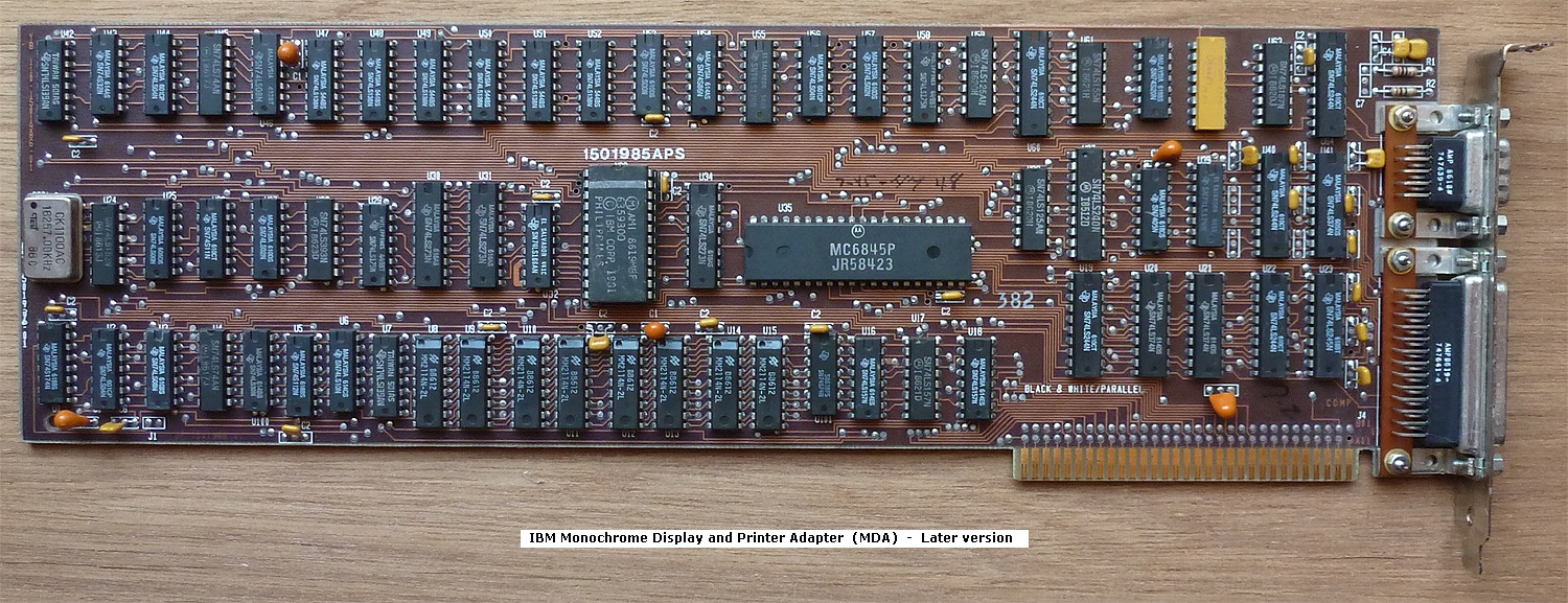
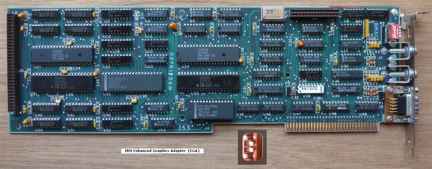
 
Switches 5 and 6:   Video card type.
 5=OFF, 6=OFF: MDA (monochrome)
 5=OFF, 6=ON : CGA, at 40 column by 25 line mode
 5=ON , 6=OFF: CGA, at 80 column by 25 line mode
 5=ON , 6=ON: Cards with a BIOS expansion ROM (e.g. EGA / PGA / VGA)


 ON/ON setting is only applicable to the 10/27/82 dated BIOS revision
Switches 7 and 8:   Floppy drive count. Used if switch 1 is OFF.
 7=ON , 8=ON: 1 floppy drive
 7=OFF, 8=ON : 2 floppy drives
 7=ON , 8=OFF: 3 floppy drives
 7=OFF, 8=OFF: 4 floppy drives


Switch block SW2

Of SW1 and SW2, SW2 is the switch block closest to the edge of the motherboard.

You set the SW2 switches to the total amount of RAM fitted in the 5150 (that is, RAM on motherboard + RAM on expansion cards).

It is important to realise that slightly different settings apply to SW2 dependent on the revision level of the BIOS in the 5150.
You can determine the BIOS revision level (a date) by looking at the seven digit number found printed on chip U33, the BIOS chip.

1. Dated 04/24/81. Chip U33 has "5700051" printed on it.
2. Dated 10/19/81. Chip U33 has "5700671" printed on it.
3. Dated 10/27/82. Chip U33 has "1501476" printed on it.

Switch settings: For the 04/24/81 and 10/19/81 BIOS, refer to pages 2-28 through 2-30 in the AUG81 edition of the Technical Reference manual.
Switch settings: For the 10/27/82 BIOS, refer to pages 5-33 through 5-50 in the APR84 edition of the Guide To Operations manual.