|
Control Word Register
|
CONTROL BYTE D7 - D0
|
|
D7
|
D6
|
D5
|
D4
|
D3
|
D2
|
D1
|
D0
|
|
SC1
|
SC0
|
RL1
|
RL0
|
M2
|
M1
|
M0
|
BCP
|
|
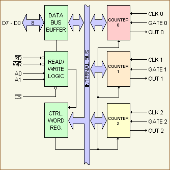
All of the operating modes for the counters are selected by writing
bytes to the control register. This is the control word format.
|
|
D7
SC1
|
D6
SC0
|
Counter Select
|
|
0
|
0
|
counter 0
|
|
0
|
1
|
counter 1
|
|
1
|
0
|
counter 2
|
|
1
|
1
|
illegal value
|
|
Bits D7 and D6 are labeled SC1 and SC0. These bits select the
counter to be programmed, it is necessary to define, using the
control bits D7 and D6, which counter is being set up.
 Once a counter is set up, it will remain that way until it is
changed by another control word.
Once a counter is set up, it will remain that way until it is
changed by another control word.
|
|
D5
RL1
|
D4
RL0
|
R / L Definition |
|
0
|
0
|
Counter value is latched. This means
that the selected counter has its
contents transferred into a temporary
latch, which can then be read by the CPU. |
|
0
|
1
|
Read / load least-significant byte only. |
|
1
|
0
|
Read / load most-significant byte only. |
|
1
|
1
|
Read / load least-significant byte first,
then most-significant byte. |
|
| |
Bits D5 and D4 ( RL1 / RL0 ) of the control word
shown above are defined as the read / load mode for the register that
is selected by bits D7 and D6. Bits D5 and D4 define how the particular
counter is to have data read from or written to it by the CPU.
These bits are defined as:
The 1st value, $00, is the counter latch mode. If this mode
is specified, the current counter value is latched into an internal
register at the time of the I/O write operation to the control register.
When a read of the counter occurs, it is this latched value that is
read.
Caution: If the latch mode is not used, then it is possible
that the data read back may be in the process of changing while the
read is occurring. This could result in invalid data being input by
the CPU ( see the timing diagrams to the 8253
by intel's site or go to page "Memory
mapped I/O" ). To read the counter value while the counter
is still in the process of counting, one must first issue a latch control
word, and then issue another control word that indicates the order of
the bytes to be read.
An alternative method of obtaining a stable count from the timer is
to externally inhibit counting while the register is being read. To
this, an external logic to the 8253 controlled by the Z80 to inhibit
count during an input read operation is to connect.
Each technique has certain disadvantages. The first, the latching method,
may give the CPU a reading that is "old" by several cycles, depending
on the speed of the count and which byte of the counter is being read.
The second method, the external inhibiting function, requires additional
hardware. In addition, it may change the overall system operation. The
counters 1 and 2 of the MZ-700 are not designed with this additional
hardware function. :-( but the counter 0. You can use this method for
your own purposes even an amplifier is connected to the output pin of
this counter.
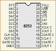
The
input to counter 0 is 1.1088MHz.
The next 3 bits of the control word are
D3, D2, and D1. These bits determine the basic mode of operation for
the selected counter. The mode descriptions follows:
|
D3
M2
|
D2
M1
|
D1
M0
|
Mode value |
|
0
|
0
|
0
|
mode 0: interrupt on terminal count |
|
0
|
0
|
1
|
mode 1: programmable one-shot |
|
x
|
1
|
0
|
mode 2: rate generator |
|
x
|
1
|
1
|
mode 3: square wave generator |
|
1
|
0
|
0
|
mode 4: software triggered strobe |
|
1
|
0
|
1
|
mode 5: hardware triggered strobe |
|
|
D0
|
counts down in
|
|
0
|
binary
|
|
1
|
BCD
|
|
The final bit D0 of the control register determines how
the register will count:
The maximum values for the count in each count mode are
104 ( 10,000 decimal ) in BCD, and 216 (
65,536 decimal ) in binary.
|
|
|
Modes
The following text describes all possible modes. The modes used in
the MZ-700 and set by the monitor's startup are mode 0, mode 2, and
mode 3.
| Mode 0 |
Interrupt on Terminal Count
The counter will be programmed to an initial value and afterwards
counts down at a rate equal to the input clock frequency. When
the count is equal to 0, the OUT pin will be a logical 1. The
output will stay a logical 1 until the counter is reloaded with
a new value or the same value or until a mode word is written
to the device.
Once the counter starts counting down, the GATE input can disable
the internal counting by setting the GATE to a logical 0 ( see
the table above ).
|
| Mode 1 |
Programmable One-Shot
In mode 1, the device can be setup to give an output pulse that
is an integer number of clock pulses. The one-shot is triggered
on the rising edge of the GATE input. If the
trigger occurs during the pulse output, the 8253 will be retriggered
again.
|
| Mode 2 |
Rate Generator
The counter that is programmed for mode 2 becomes a "divide by
n" counter. The OUT pin of the counter goes to low for one input
clock period. The time between the pulses of going low is dependent
on the present count in the counter's register. I mean the time
of the logical 1 pulse.
For example, suppose to get an output frequency of 1,000 Hz (
Hertz ), the period would be 1 / 1,000 s = 1 ms ( millisecond
) or 1,000 µs ( microseconds ). If an input clock of 1 MHz
( Mega-Hertz ) were applied to the clock input of the counter
#0, then the counter #0 would need to be programmed to 1000 µs.
This could be done in decimal or in BCD. ( The period of an input
clock of 1 MHz is 1 / 1,000,000 = 1 µs. )
The formula is: n=fi divided by fout.
fi = input clock frequency, fout = output
frequency, n = value to be loaded.
My example: fi = 1 MHz = 1 x 10⁶ Hz, fout
= 1 kHz = 1 x 10³ Hz.
n = 1 x 10⁶ Hz / 1 x 10³ Hz = 1 x 103
= 1,000. This is the decimal value to be loaded or the hexadecimal
value $03E8. The following program example uses the decimal load
count.
B000 3E35	LD	A,$35     ; load control word
			          ; for counter 0 mode 2
B002 3207E0	LD	($E007),A ; into port $E007
                                  ; for BCD count
B005 2104E0	LD	HL,$E004  ; address to the port
                                  ; of counter 0
B008 3E00	LD	A,$00
B00A 77		LD	(HL),A	  ; load least significant
                                  ; byte of 1000 first
B00B 3E10	LD	A,$10
B00D 77		LD	(HL),A	  ; load most significant
                                  ; byte of 1000 last
B00E 3E01	LD	A,1
B010 3208E0	LD	($E008),A ; start counter 0 is only
                                  ; necessary for the MZ-700.
                                  ; Not necessary for
                                  ; counter #1 and #2
;
; The counter is now initialized and the output frequency
; will be 1000 Hz if the input frequency is 1 MHz.
If the count is loaded between output pulses, the present period
will not be affected. A new period will occur during the next
count sequence.
|
| Mode 3 |
Square Wave Generator
Mode 3 is similar to the mode 2 except that the output will be
high for half the period and low for half. If the count is odd,
the output will be high for ( n + 1 ) / 2 and low for ( n - 1
) / 2 counts.
For example, I'll setup counter #0 for a square wave frequency
of 10 kHz ( kilo-Hertz ), assuming the input frequency is 1 MHz.
Please refer to the formula described at mode 2.
1 x 10⁶ / 10 x 103 = 100. This is the decimal
value to be loaded or the hexadecimal value $0064. The following
program example uses the binary load count.
B000 3E35	LD	A,$36	  ; load control word
			          ; for counter 0 mode 3
B002 3207E0	LD	($E007),A ; into port $E007
                                  ; for binary count
B005 2104E0	LD	HL,$E004  ; address to the port
                          ; of counter 0
B008 3E00	LD	A,$64	  ; equals to
                                  ; 100 microseconds
                                  ; for 10,000 Hz
B00A 77		LD	(HL),A	  ; load least significant
                                  ; byte of $0064 first
B00B 3E10	LD	A,$00
B00D 77		LD	(HL),A	  ; load most significant
                                  ; nyte of $0064 last
B00E 3E01	LD	A,1
B010 3208E0	LD	($E008),A ; start counter 0 is only
				  ; necessary for the MZ-700.
                  ; Not necessary for counter
                                  ; #1 and #2
;
; The counter is now initialized and the output frequency
; will be 10 kHz if the input frequency is 1 MHz.
|
| Mode 4 |
Software Triggered Strobe
In this mode the programmer can set up the counter to give an
output timeout starting when the register is loaded. On the terminal
count, when the counter equals to 0, the output will go to a logical
0 for one clock period and then returns to a logical 1. First
the mode is set, the output will be a logical 1.
|
| Mode 5 |
Hardware Triggered Strobe
In this mode the rising edge of the trigger input will start
the counting of the counter. The output goes low for one clock
at the terminal count. The counter is retriggerable, thus meaning
that if the trigger input is taken low and then high during a
count sequence, the sequence will start over.
When the external trigger input goes to a logical 1, the timer
will start to time out. If the external trigger occurs again,
prior to the time completing a full timeout, the timer will retrigger.
|
Go to page "Memory mapped I/O" to
download the complex datasheet of the 8253.
|